

Fairchild Semiconductor NC7SZ86 Datasheet
NC7SZ86
NC7SZ86 TinyLogic
October 1996
Revised May 2003
TinyLogic
General Description
The NC7SZ86 is a single 2-I nput Exclusive- OR Gate from
Fairchild’s Ultra High Speed Series of TinyLogic
device is fabricated wi th advanced CMOS technology to
achieve ultra high spe ed w ith h i gh out put drive while mai ntaining low static power dissipation over a very broad V
operating range. Th e device is specified to operate ov er
the 1.65V to 5.5V V
high impedance when V
up to 6V independent of V
UHS 2-Input Exclusive-OR Gate
Features
■ Space saving SOT23 or SC70 5-lead package
■ Ultra small MicroPak
■ Ultra High Speed; t
■ High Output Drive; ± 24 mA at 3V V
CC
■ Broad VCC Operating Range; 1.65V to 5.5V
■ Matches the performance of LCX when operated at 3.3V
■ Power down high impedance inputs/output
■ Overvoltage tolerant inputs facilitate 5V to 3V translation
■ Patented noise/EMI reduction circuitry implemented
leadless package
2.9 ns typ into 50 pF at 5V V
PD
range. The in puts and output are
CC
is 0V. Inputs tolerate voltages
CC
operating voltage.
CC
. The
CC
CC
Ordering Code:
Order Package Product Code
Number Number Top Mark
NC7SZ86M5X MA05B 7Z86 5-Lead SOT23, JEDEC MO-178, 1.6mm 3k Units on Tape and Reel
NC7SZ86P5X MAA05A Z86 5-Lead SC70, EIAJ SC-88a, 1.25mm Wide 3k Units on Tape and Reel
NC7SZ86L6X MAC06A B3 6-Lead MicroPak, 1.0mm Wide 5k Units on Tape and Reel
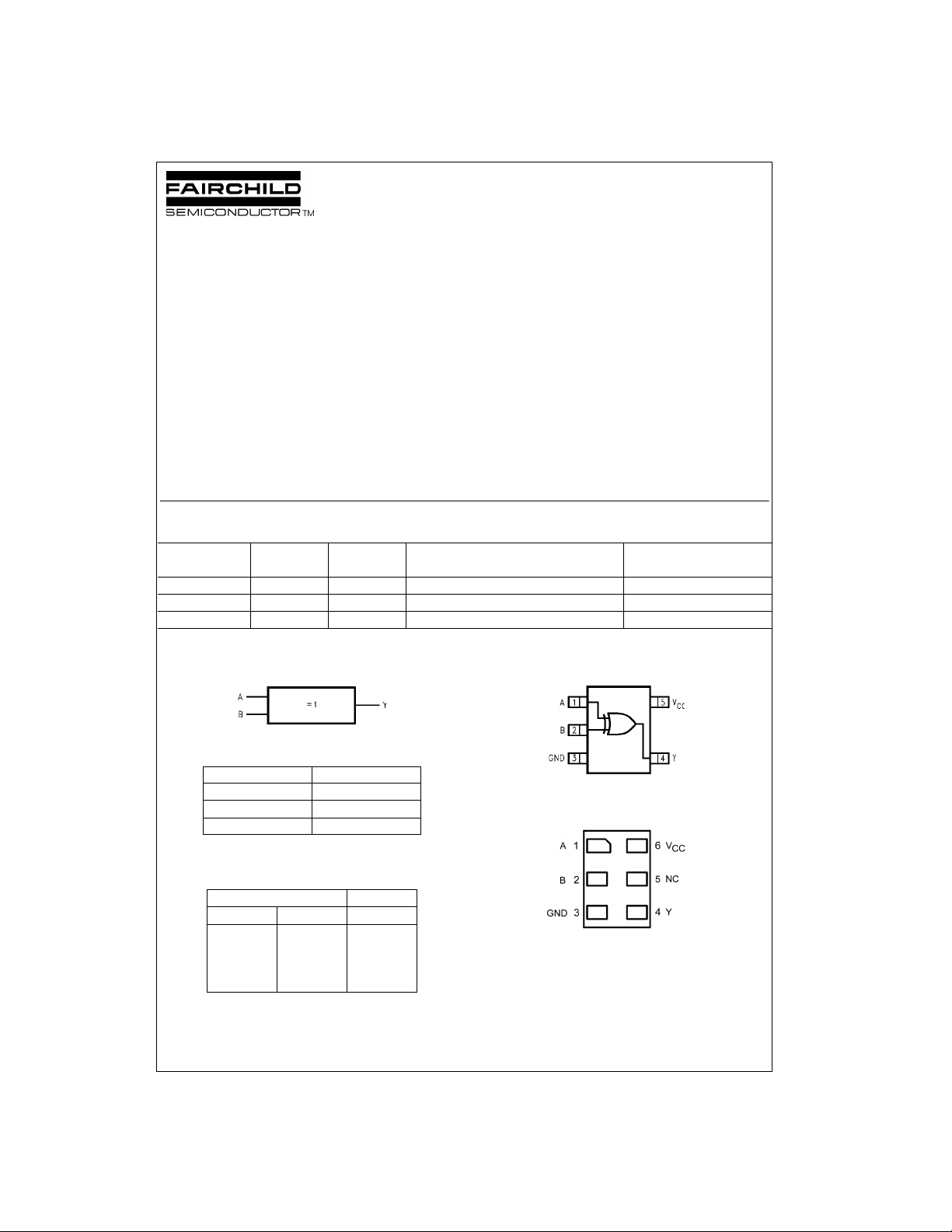
Logic Symbol
IEEE/IEC
Package Descript ion Supplied As
Connection Diagrams
Pin Assignme nts for SC70 and SOT23
UHS 2-Input Exclusive-OR Gate
Pin Descriptions
Pin Names Description
A, B Input
Y Output
NC No Connect
Pad Assignments for MicroPak
(Top View)
Function Table
Y = A⊕B
Inputs Output
ABY
LLL
LHH
HLH
HHL
H = HIGH Logic Le v el L = LOW Logic Lev el
TinyLogic is a registered trademark of F airc hild Semiconduct or Corporation.
MicroPak is a tradem ark of Fairchild Semiconductor Corporation.
© 2003 Fairchild Semiconductor Corporation DS012164 www.fairchildsemi.com
(Top Thru View)
Absolute Maximum Ratings(Note 1) Recommended Operating
Supply Voltage (VCC) −0.5V to +6V
DC Input Voltage (V
NC7SZ86
DC Output Voltage (V
DC Input Diode Current (I
@V
< −0.5V −50 mA
IN
@ V
> 6V +20 mA
IN
DC Output Diode Current (I
@V
< −0.5V −50 mA
OUT
@ V
> 6V, VCC = GND +20 mA
OUT
DC Output Current (I
DC V
/GND Current (ICC/I
CC
Storage Temperature (T
Junction Temperature under Bias (T
Junction Lead Temperature (T
) −0.5V to +6V
IN
) −0.5V to +6V
OUT
)
IK
)
OK
) ± 50 mA
OUT
) ± 50 mA
GND
) −65°C–+150°C
STG
) 150°C
J
);
L
(Soldering, 10 seconds) 260
Power Dissipation (P
) @ +85°C
D
SOT23-5 200 mW
SC70-5 150 mW
Conditions
Supply Voltage Operating (V
Supply Voltage Data Retention (V
Input Voltage (V
Output Voltage (V
Operating Temperature (TA) −40°C–+85°C
Input Rise and Fall Time (t
= 1.8V, 2.5V ±0.2V 0 ns/V–20 ns/V
V
CC
V
= 3.3V ± 0.3V 0 ns/V–10 ns/V
CC
V
= 5.0V ± 0.5V 0 ns/V–5 ns/V
CC
Thermal Resistance (
SOT23-5 300
SC70-5 425
Note 1: Absolute maximum ratings are DC values beyond which the devi ce
°C
may be damage d or h ave its us eful life im pai red. Th e dat as heet sp ecific ations should be met, without exception, to ensure that the system design is
reliable over its power supply, temperature, and output/input loading variables. Fairchild does no t recommend operation outsid e datasheet spec ifications.
Note 2: Unused inputs must be held HIGH or LOW. They may not float.
(Note 2)
) 1.65V to 5.5V
CC
)0V to 5.5V
IN
) 0V to V
OUT
, tf)
r
θ
)
JA
DC Electrical Characteristics
V
Symbol Parameter
V
HIGH Level Input Voltage 1.65 to 1.95 0.75 V
IH
V
LOW Level Input Vo ltage 1.65 to 1.95 0.25 V
IL
V
HIGH Level Output Voltage 1.65 1.55 1.65 1.55
OH
V
LOW Level Output Voltage 1.65 0.0 0.1 0.1
OL
I
Input Leakage Current 0 to 5.5 ±1 ±10 µAVIN = 5.5V, GND
IN
I
Power Off Leakage Current 0.0 1 10 µAVIN or V
OFF
I
Quiescent Supply Current 1.65 to 5.5 2.0 20 µAVIN = 5.5V, GND
CC
CC
(V) Min T yp Max Min Max
2.3 to 5.5 0.7 V
2.3 to 5.5 0.3 V
1.8 1.7 1.8 1.7
2.3 2.2 2.3 2.2
3.0 2.9 3.0 2.9
4.5 4.4 4.5 4.4
1.65 1.29 1.52 1.29
2.3 1.9 2.15 1.9 I
3.0 2.4 2.80 2.4 IOH = −16 mA
3.0 2.3 2.68 2.3 IOH = −24 mA
4.5 3.8 4.20 3.8 IOH = −32 mA
1.8 0.0 0.1 0.1
2.3 0.0 0.1 0.1
3.0 0.0 0.1 0.1
4.5 0.0 0.1 0.1
1.65 0.08 0.24 0.24
2.3 0.10 0.3 0.3 IOL = 8 mA
3.0 0.15 0.4 0.4 IOL = 16 mA
3.0 0.22 0.55 0.55 IOL = 24 mA
4.5 0.22 0.55 0.55 IOL = 32 mA
TA = +25°CT
CC
CC
A
0.75 V
0.7 V
CC
CC
= −40°C to +85°C
CC
CC
0.25 V
0.3 V
CC
Units Conditions
V
CC
V
VV
V
VVIN = VIH or VILIOL = 100 µA
V
) 1.5V to 5.5V
CC
= VIH, VILIOH = −100 µA
IN
IOH = −4 mA
= −8 mA
OH
IOL = 4 mA
= 5.5V
OUT
CC
°C/W
°C/W
www.fairchildsemi.com 2
AC Electrical Characteristics
V
Symbol Parameter
CC
(V) Min Typ Max Min Max Number
1.65 2.0 6.9 13.8 2.0 14.5
t
, Propagation Delay 1.8 2.0 5.7 11.5 2.0 12
PLH
t
PHL
2.5 ± 0.2 0.8 3.8 8.0 0.8 8.5 CL = 15 pF,
3.3 ± 0.3 0.5 3.0 5.7 0.5 6.0 R
5.0 ± 0.5 0.5 2.4 5.0 0.5 5.4
t
t
C
C
PLH,
PHL
Propagation Delay 3.3 ± 0.3 1.5 3.5 6.2 1.5 6.5
5.0 ± 0.5 0.8 2.9 5.4 1.0 5.8 RL = 500Ω
Input Capacitance 0 4 pF
IN
Power Dissipation Capacitance 3.3 25
PD
5.0 31
Note 3: CPD is defined as the value of the internal equivalent capacitance which is derived from dynamic operating current consumption (I
loading and operating at 50% duty cycle. (See Figure 2.) C
I
= (CPD)(VCC)(fIN) + (ICCstatic).
CCD
PD
TA = +25°CT
is related to I
dynamic operating current by the express ion:
CCD
= −40°C to +85°C
A
Units Conditions
ns
ns
pF (Note 3) Figure 2
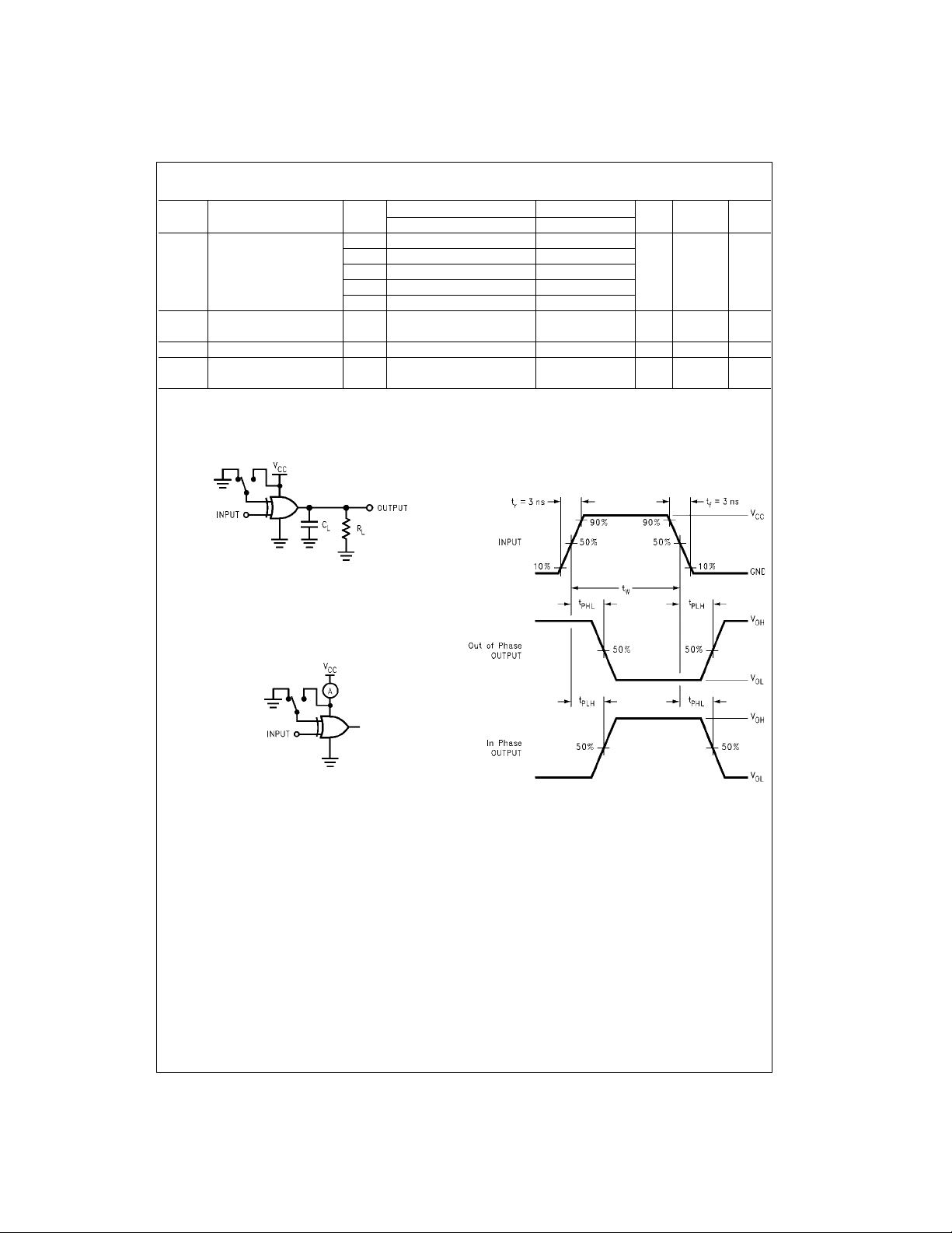
AC Loading and Waveforms
CL includes load and s tr ay c apacitance
Input PR R = 1.0 MHz; t
= 500 ns
w
FIGURE 1. AC Test Circuit
= 1 MΩ
L
CL = 50 pF,
) at no output
CCD
Figure
Figures
1, 3
Figures
1, 3
NC7SZ86
Input = AC Wavefor m; tr = tf = 1.8 ns;
PRR = 10 MHz; Duty Cycle = 50%
FIGURE 2. I
Test Circuit
CCD
FIGURE 3. AC Waveforms
3 www.fairchildsemi.com
 Loading...