Fairchild Semiconductor NC7SZ66 Datasheet

NC7SZ66
NC7SZ66 TinyLogic
November 1996
Revised August 2003
TinyLogic
Low Voltage UHS Single SPST
Normally Open Bus Switch
General Description
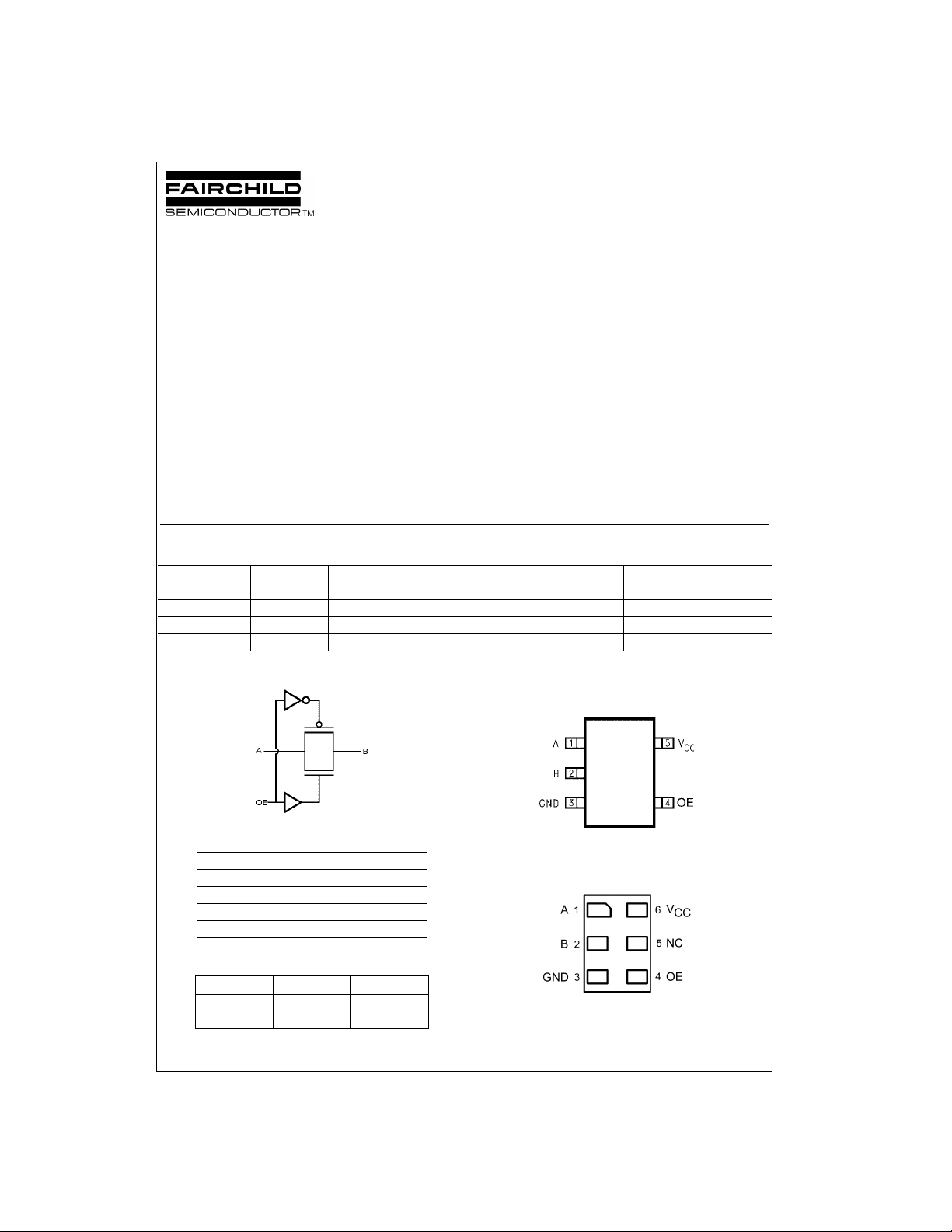
The NC7SZ66 is a ultra high-speed (UHS) CMOS compatible single-pole/single-throw (SPST) bus switch. The LOW
On Resistance of the switch all ows input s to be conn ect ed
to outputs with minimal propagation delay and without generating additional ground bounce noise. The device is
organized as a 1-bit switch with a switch enab le (OE) signal. When OE is HIGH, th e switch is on an d Por t A is co nnected to Port B. When OE is LOW, the switch is open and
a high-impedance state exists bet ween the two ports.
Ordering Code:
Order Package Product Code
Number Number Top Mark
NC7SZ66M5X MA05B 7Z66 5-Lead SOT23, JEDEC MO-178, 1.6mm 3k Units on Tape and Reel
NC7SZ66P5X MAA05A Z66 5-Lead SC70, EIAJ SC-88a, 1.25mm Wide 3k Units on Tape and Reel
NC7SZ66L6X MAC06 EE 6-Lead MicroPak, 1.0mm Wide 5k Units on Tape and Reel
Logic Symbol
Features
■ Space saving SOT23 or SC70 5-lead package
■ Ultra small MicroPak
■ Broad V
■ Rail-to-rail signal handling
■ 5
■ Minimal propagation delay through the switch
■ Low I
■ Zero bounce in flow-through mode
■ Control input compatible with CMOS input levels
Package Descript ion Supplied As
Operating Range 1.65V–5.5V
CC
Ω switch connection between two ports
CC
leadless package
Connection Diagrams
Pin Assignments for SC 70
Low Voltage UHS Single SPST Normally Open Bus Switch
Pin Descriptions
Pin Names Description
OE Switch Enable Input
A Bus A I/O
B Bus B I/O
NC No Connect
Pad Assignment for MicroPak
(Top View)
Function Table
OE B
L HIGH-Z State Disconnect
HA
TinyLogic is a registered tradema rk of F airc hild Semiconduct or Corporation.
MicroPak is a tradem ark of Fairchild Semiconductor Corporation.
© 2003 Fairchild Semiconductor Corporation DS012177 www.fairchildsemi.com
0
0
Function
Connect
(Top Through View)

Absolute Maximum Ratings(Note 1) Recommended Operating
Supply Voltage (VCC) −0.5V to +7.0V
DC Switch Voltage (V
NC7SZ66
DC Input Voltage (V
) −0.5V to VCC +0.5V
S
) (Note 2) −0.5V to +7.0V
IN
DC Input Diode Current
) VIN < 0V −50 mA
(I
IK
DC Output (I
DC V
CC
) Sink Current 128 mA
OUT
/GND Current (ICC/I
) ±100 mA
GND
Storage Temperature Range
(T
) −65°C to +150°C
STG
Junction Lead Temperature
under Bias (T
Junction Lead Temperature (T
) +150°C
J
)
L
(Soldering, 10 Second s)
Power Dissipation (P
) @ +85°C
D
SOT23-5 200 mW
SC70-5 150 mW
+260°C
Conditions
Power Supply Operating (V
Control Input Voltage (V
Switch Input Voltage (V
Switch Output Voltage (V
Input Rise and Fall Time (tr, tf)
Control Input; V
Control Input; V
Switch I/O 0 ns/V to DC
Operating Temperature (T
Thermal Resistance (
SOT23-5 300
SC70-5 425
Note 1: The “Absolute Maximum Ratings” are those values bey ond which
the safety of the d evice cannot be guaranteed. The device sh ould not be
operated at these limit s. The parametric values defin ed in the Electrical
Characteristics tables are not guaranteed at the absolute maximum ratings.
The “Recomme nded O peratin g Cond itions ” table will defin e the condition s
for actual device operation.
Note 2: The input and output ne gative vo ltage ra tings may be excee ded if
the input and output diode current ratings are observed.
Note 3: Unused inputs must be held HIGH or LOW. They may not float.
(Note 3)
) 1.65V to 5.5V
CC
) 0V to 5.5V
IN
)0V to V
IN
)0V to V
OUT
= 2.3V−3.6V 0 ns/V to 10 ns
CC
= 4.5−5.5V 0 ns/V to 5 ns
CC
) −40°C to +85°C
A
θ
)
JA
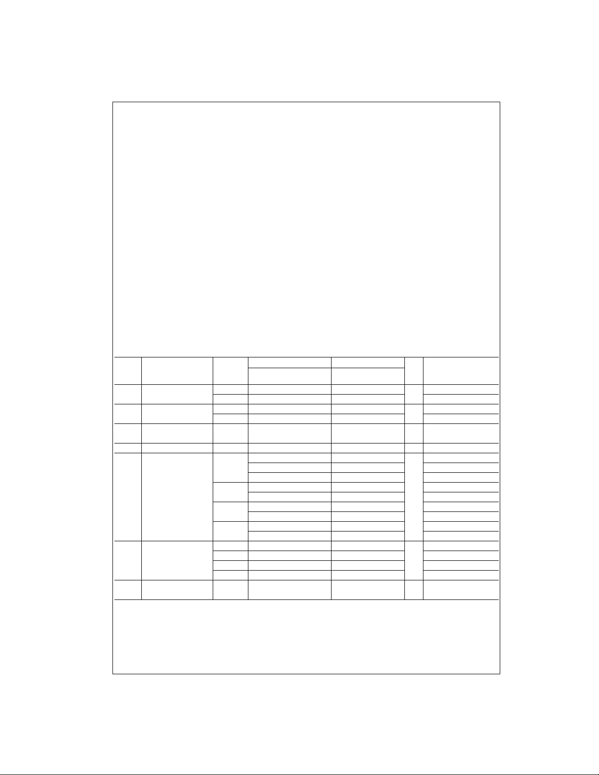
DC Electrical Characteristics
V
Symbol Parameter
V
HIGH Level 1.65 to 1.95 0.75 V
IH
Input Voltage 2.3 to 5.5 0.7 V
V
LOW Level 1.65 to 1.95 0.25 V
IL
Input Voltage 2.3 to 5.5 0.3 V
I
Control Input
IN
Leakage Current
I
OFF Leakage Current 1.65 to 5.5 ±0.05 ±10.0 µA0 ≤ A, B ≤ V
OFF
R
Switch On Resistance
ON
(Note 4) 5 12 VIN = 2.4V, IIN = 15 mA
R
On Resistance Flatness 5.0 6
flat
(Note 4)(Note 6)(Note 7) 3.3 12 IA = −24 mA, 0 ≤ VBn ≤ V
I
Quiescent Supply Current
CC
Note 4: Measured by the volta ge drop between A an d B pins at the indicated c urrent through the switch. On Resistance is determined by the lower of the
voltages on the two (A or B) pins.
Note 5: All typical values are at the specified V
Note 6: Parameter is characterized but not tested in production.
Note 7: Flatness is defined as th e difference between the maximum and minimum value of On Res is t ance over the specifi ed range of conditions.
CC
(V) Min Typ
0 to 5.5 ±0.05 ±1.0 µA0 ≤ V
4.5
3.0
2.3
1.8
2.5 28 IA = −8 mA, 0 ≤ VBn ≤ V
1.8 125 IA = −4 mA, 0 ≤ VBn ≤ V
1.65 to 5.5 0.05 10 µA
CC
TA= −40°C to +85°CT
(Note 5)
CC
CC
, and TA = 25°C.
Max Min Typ Max
CC
CC
37
715 V
49 V
10 20 VIN = 3V, IIN = 24 mA
512 VIN = 0V, IIN = 8 mA
13 30 VIN = 2.3V, IIN = 8 mA
728 VIN = 0V, IIN = 4 mA
25 60 VIN = 1.8V, IIN = 4 mA
= +25°C
A
Units Conditions
V
V
≤ 5.5V
IN
VIN = 0V, IIN = 30 mA
= 4.5V, IIN = 30 mA
IN
= 0V, IIN = 24 mA
IN
Ω
IA = −30 mA, 0 ≤ VBn ≤ V
Ω
VIN = VCC or GND
I
= 0
OUT
CC
CC
°C/Watt
°C/Watt
CC
CC
CC
CC
CC
www.fairchildsemi.com 2

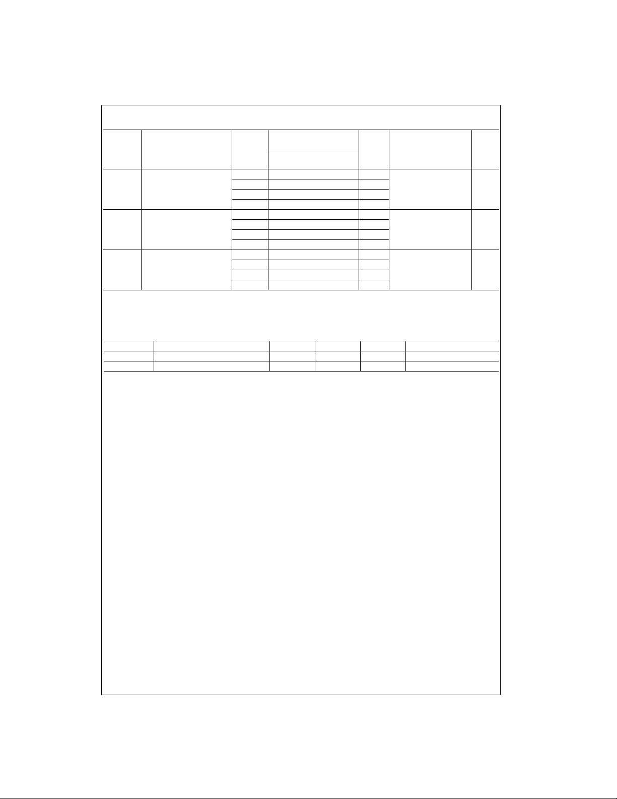
AC Electrical Characteristics
TA= −40°C to +85°C,
Symbol Parameter
, t
t
PHL
Propagation Delay Bus to Bus 1.65 to 1.95 4.3
PLH
V
(V) Min Typ
CL= 50 pF, RU= RD = 500Ω
CC
(Note 8)
Units Conditions Figure
Max Number
(Note 9) 2.3-2.7 1.2 ns VIN = OPEN
3.0-3.6 0.8 ns
4.5-5.5 0.3 ns
t
, t
PZL
Output Enable Time 1.65 to 1.95 1.5 7.0 14.2
PZH
2.3-2.7 1.5 3.3 7.0 ns V
3.0-3.6 1.5 2.4 5.5 ns VIN = 0V for t
= 2 x VCC for t
IN
PZL
PZH
4.5-5.5 1.5 2.0 4.5 ns
t
, t
PLZ
Output Disable Time 1.65 to 1.95 1.5 9.2 18.2
PHZ
2.3-2.7 1.5 5.3 9.0 ns V
3.0-3.6 1.5 4.0 7.0 ns VIN = 0V for t
= 2 x VCC for t
IN
PLZ
PHZ
4.5-5.5 1.5 2.7 5.0 ns
Note 8: All typical values are at the s pec ified VCC, and TA = 25°C.
Note 9: This parameter is guaranteed by design but is not tested. The switch contributes no propagation delay other than the RC delay of the typical On
Resistance of the switch and the 50 pF load ca pacitance, when driv en by an ideal voltage s ource (zero output imp edance).
Capacitance
Symbol Parameter Typ Max Units Conditions
C
IN
C
I/O
Control Pin Input Capacitance 2 pF VCC = 0V
Input/Output Capacitance 6 pF VCC = 5.0V
Figures
1, 2
Figures
1, 2
Figures
1, 2
NC7SZ66
3 www.fairchildsemi.com
 Loading...