

Fairchild Semiconductor NC7SZ386 Datasheet
NC7SZ386
NC7SZ386 TinyLogic
June 2001
Revised April 2003
TinyLogic
General Description
The NC7SZ386 is a single 3-Input Exclusive-OR Gate from
Fairchild’s Ultra High Speed Series of TinyLogic
device is fabricated wi th advanced CMOS technology to
achieve ultra high spe ed w ith h i gh out put drive while mai ntaining low static power dissipation over a very broad V
operating range. Th e device is specified to operate ov er
the 1.65V to 5.5V V
high impedance when V
up to 7V independent of V
UHS 3-Input Exclusive-OR Gate
Features
■ Space saving SC70 6-lead package
■ Ultra small MicroPak
■ Ultra High Speed; t
■ High Output Drive; ± 24 mA at 3V V
CC
■ Broad VCC Operating Range; 1.65V to 5.5V
■ Power down high impedance inputs/output
■ Overvoltage tolerant inputs facilitate 5V to 3V translation
■ Patented noise/EMI reduction circuitry implemented
leadless package
2.9 ns typ into 50 pF at 5V V
PD
range. The in puts and output are
CC
is 0V. Inputs tolerate voltages
CC
operating voltage.
CC
. The
CC
CC
Ordering Code:
Order Package Product Code
Number Number Top Mark
NC7SZ386P6X MAA06A 386 6-Lead SC70, EIAJ SC88, 1.25mm Wide 3k Units on Tape and Reel
NC7SZ386L6X MAC06A F4 6-Lead MicroPak, 1.0mm Wide 5k Units on Tape and Reel
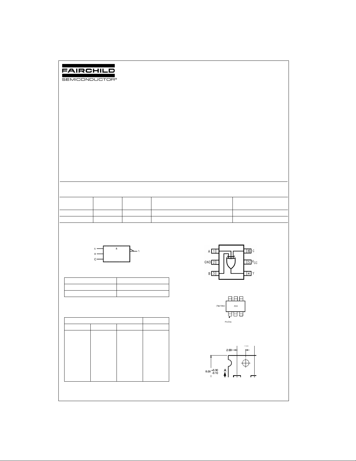
Logic Symbol
IEEE/IEC
Package Description Supplied As
Connection Diagrams
Pin Assignments for SC 70
Pin Descriptions
Pin Names Description
A, B, C Input
YOutput
Pin One Orientation Diagram
(Top View)
UHS 3-Input Exclusive-OR Gate
Function Table
Y = A ⊕ B ⊕ C
Inputs Output
ABCY
LLLL
LLHH
LHLH
LHHL
HLLH
HLHL
HHL L
HHHH
H = HIGH Logic Le v el L = LOW Logic Level
TinyLogic is a registered trademark of F airc hild Semiconduct or Corporation.
MicroPak is a tradem ark of Fairchild Semiconductor Corporation.
© 2003 Fairchild Semiconductor Corporation DS500468 www.fairchildsemi.com
AAA represents Product Code Top Mark - see ordering code
Note: Orie ntation of Top Mark determines Pin On e locat ion. Rea d the Top
Product Code Mark left to right, Pin One is the lower left pin (see diagram).
Pad Assignments for MicroPak
(Top Thru View)
Absolute Maximum Ratings(Note 1) Recommended Operating
Supply Voltage (VCC) −0.5V to +6V
DC Input Voltage (V
DC Output Voltage (V
NC7SZ386
DC Input Diode Current (I
@V
< −0.5V −50 mA
IN
@ V
> 6V +20 mA
IN
DC Output Diode Current (I
@V
< −0.5V −50 mA
OUT
@ V
> 6V, VCC = GND +20 mA
OUT
DC Output Current (I
DC V
/GND Current (ICC/I
CC
Storage Temperature (T
Junction Temperature under Bias (T
Junction Lead Temperature (T
) −0.5V to +6V
IN
) −0.5V to +6V
OUT
)
IK
)
OK
) ± 50 mA
OUT
) ± 50 mA
GND
) −65°C to +150°C
STG
) 150°C
J
);
L
(Soldering, 10 seconds) 260
Power Dissipation (P
) @ +85°C
D
SC70-5 150 mW
Conditions
Supply Voltage Operating (V
Supply Voltage Data Retention (V
Input Voltage (V
Output Voltage (V
Operating Temperature (TA) −40°C to +85°C
Input Rise and Fall Time (t
= 1.8V, 2.5V ±0.2V 0 ns/V to 20 ns/V
V
CC
V
= 3.3V ± 0.3V 0 ns/V to 10 ns/V
CC
V
= 5.0V ± 0.5V 0 ns/V to 5 ns/V
CC
Thermal Resistance (
SC70-5 425
Note 1: Absolute maximum ratings are DC values beyond which the devi ce
may be damage d or h ave its us eful life im pai red. Th e dat as heet sp ecific a-
°C
tions should be met, without exception, to ensure that the system design is
reliable over its power supply, temperature, and output/input loading variables. Fairchild does no t recommend operation outsid e datasheet spec ifications.
Note 2: Unused inputs must be held HIGH or LOW. They may not float.
(Note 2)
) 1.65V to 5.5V
CC
)0V to 5.5V
IN
) 0V to V
OUT
, tf)
r
θ
)
JA
DC Electrical Characteristics
V
Symbol Parameter
V
HIGH Level Input Voltage 1.8 ± 0.15 0.75 V
IH
V
LOW Level Input Voltage 1.8 ± 0.15 0.25 V
IL
V
HIGH Level Output Voltage 1.65 1.55 1.65 1.55
OH
V
LOW Level Output Voltage 1.65 0.0 0.1 0.1
OL
I
Input Leakage Current 0 to 5.5 ±1 ±10 µAVIN = 5.5V, GND
IN
I
Power Off Leakage Current 0.0 1 10 µAVIN or V
OFF
I
Quiescent Supply Current 1.65 to 5.5 2.0 20 µAVIN = 5.5V, GND
CC
CC
(V) MinTypMaxMinMax
2.3 to 5.5 0.7 V
2.3 to 5.5 0.3 V
2.3 2.2 2.3 2.2
3.0 2.9 3.0 2.9
4.5 4.4 4.5 4.4
1.65 1.29 1.52 1.29 I
2.3 1.9 2.15 1.9 I
3.0 2.4 2.80 2.4 IOH = −16 mA
3.0 2.3 2.68 2.3 I
4.5 3.8 4.20 3.8 I
2.3 0.0 0.1 0.1
3.0 0.0 0.1 0.1
4.5 0.0 0.1 0.1
1.65 0.08 0.24 0.24 IOL = 4 mA
2.3 0.10 0.3 0.3 IOL = 8 mA
3.0 0.15 0.4 0.4 IOL = 16 mA
3.0 0.22 0.55 0.55 IOL = 24 mA
4.5 0.22 0.55 0.55 IOL = 32 mA
TA = +25°CT
CC
CC
A
0.75 V
0.7 V
CC
CC
= −40°C to +85°C
CC
CC
0.25 V
0.3 V
CC
Units Conditions
V
CC
V
V
V
) 1.5V to 5.5V
CC
CC
°C/W
VIN = VIH, VILIOH = −100 µA
= −4 mA
OH
= −8 mA
OH
= −24 mA
OH
= −32 mA
OH
VIN = VIH or VILIOL = 100 µA
= 5.5V
OUT
www.fairchildsemi.com 2
AC Electrical Characteristics
V
Symbol Parameter
t
, Propagation Delay 1.8 ± 0.15 2.0 14.0 2 2.5 2.0 23.0
PLH
t
PHL
CC
(V) Min Typ Max Min Max
2.5 ± 0.2 0.8 8.0 12.5 0.8 13.0 CL = 15 pF,
3.3 ± 0.3 0.5 6.0 9.2 0.5 9.5 R
5.0 ± 0.5 0.5 4.3 5.7 0.5 6.1
t
t
C
C
PLH,
PHL
Propagation Delay 3.3 ± 0.3 1.5 6.1 9.5 1.5 9.8
5.0 ± 0.5 0.8 4.8 6.5 1.0 6.9 RL = 500Ω
Input Capacitance 0 4 pF
IN
Power Dissipation Capacitance 3.3 25
PD
5.0 31
Note 3: CPD is defined as the value of the internal equivalent capacitance which is derived from dynamic operating current consumption (I
loading and operating at 50% duty cycle. (See Figure 2.) C
= (CPD)(VCC)(fIN) + (ICCstatic).
I
CCD
PD
TA = +25°CT
is related to I
dynamic operating current by the express ion:
CCD
= −40°C to +85°C
A
Units Conditions Fig. No.
ns
ns
pF (Note 3) Figure 2
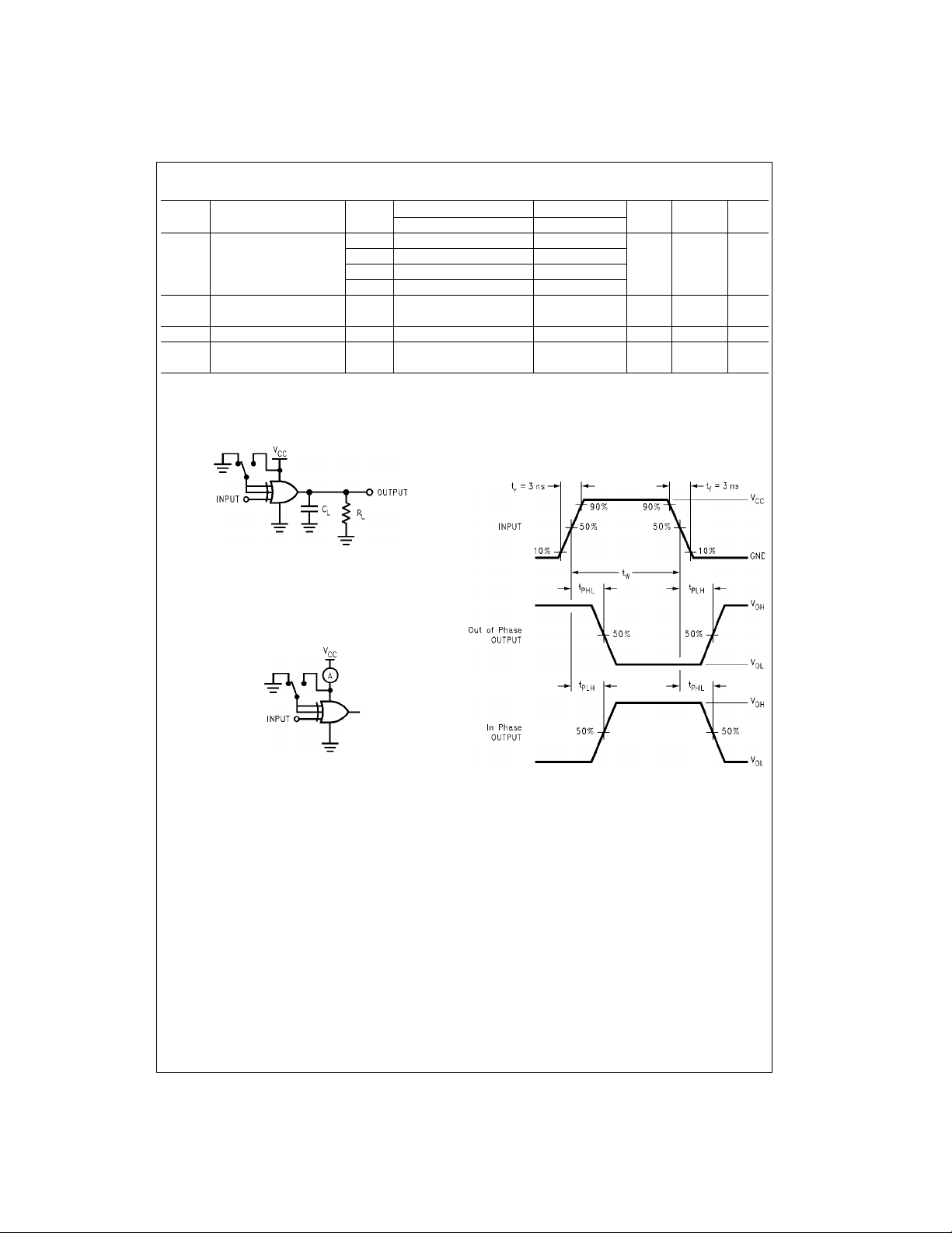
AC Loading and Waveforms
CL includes load and s tr ay c apacitance
Input PR R = 1.0 MHz; t
= 500 ns
w
FIGURE 1. AC Test Circuit
= 1 MΩ
L
CL = 50 pF,
) at no output
CCD
Figures
1, 3
Figures
1, 3
NC7SZ386
Input = AC Wavefor m; tr = tf = 1.8 ns;
PRR = 10 MHz; Duty Cycle = 50%
FIGURE 2. I
Test Circuit
CCD
FIGURE 3. AC Waveforms
3 www.fairchildsemi.com
 Loading...