

Fairchild Semiconductor NC7SZ373 Datasheet
NC7SZ373
NC7SZ373 TinyLogic
June 1998
Revised May 2003
TinyLogic
General Description
The NC7SZ373 is a s ingle positive edge -triggered D-type
CMOS Latch with 3-STATE output from Fairchild’s Ultra
High Speed Series of TinyLogic
SC70 6-lead package. The device is fabricated with
advanced CMOS technolog y to achieve ultra high speed
with high output drive while maintaining low static power
dissipation over a very broad V
device is specified to operate over the 1.65V to 5.5V range.
The inputs and output are high impedance when V
Inputs tolerate voltages up to 7V inde pe nde nt o f V
ating voltage. The latc h appears transparent to the data
when Latch Enable (LE ) is HIGH. When LE is LOW, the
data that meets the set up ti me is l a tche d. Th e o utp ut tolerates voltages above V
UHS D-Type Latch with 3-STAT E Output
Features
■ Space saving SC70 6-lead package
in the space saving
operating range. The
CC
in the 3-STATE condition.
CC
CC
CC
is 0V.
oper-
■ Ultra small MicroPak
■ Ultra High Speed; t
■ High Output Drive; ±24 mA at 3V V
■ Broad VCC Operating Range; 1.65V to 5.5V
■ Matches the performance of LCX when operated at
3.3V V
CC
■ Power down high impedance inputs/output
■ Overvoltage tolerant inputs facilitate 5V to 3V translation
■ Patented noise/EMI reduction circuitry implemented
leadless package
2.6 ns Typ into 50 pF at 5V V
PD
CC
CC
Ordering Code:
Order Package Product Code
Number Number Top Mark
NC7SZ373P6X MAA06A Z73 6-Lead SC70, EIAJ SC88, 1.25mm Wide 3k Units on Tape and Reel
NC7SZ373L6X MAC06A D4 6-Lead MicroPak, 1.0mm Wide 5k Units on Tape and Reel
Package Description Supplied As
UHS D-Type Latch with 3-STATE Output
TinyLogic is a registered tradema rk of F airc hild Semiconduct or Corporation.
MicroPak is a tradem ark of Fairchild Semiconductor Corporation.
© 2003 Fairchild Semiconductor Corporation DS500157 www.fairchildsemi.com
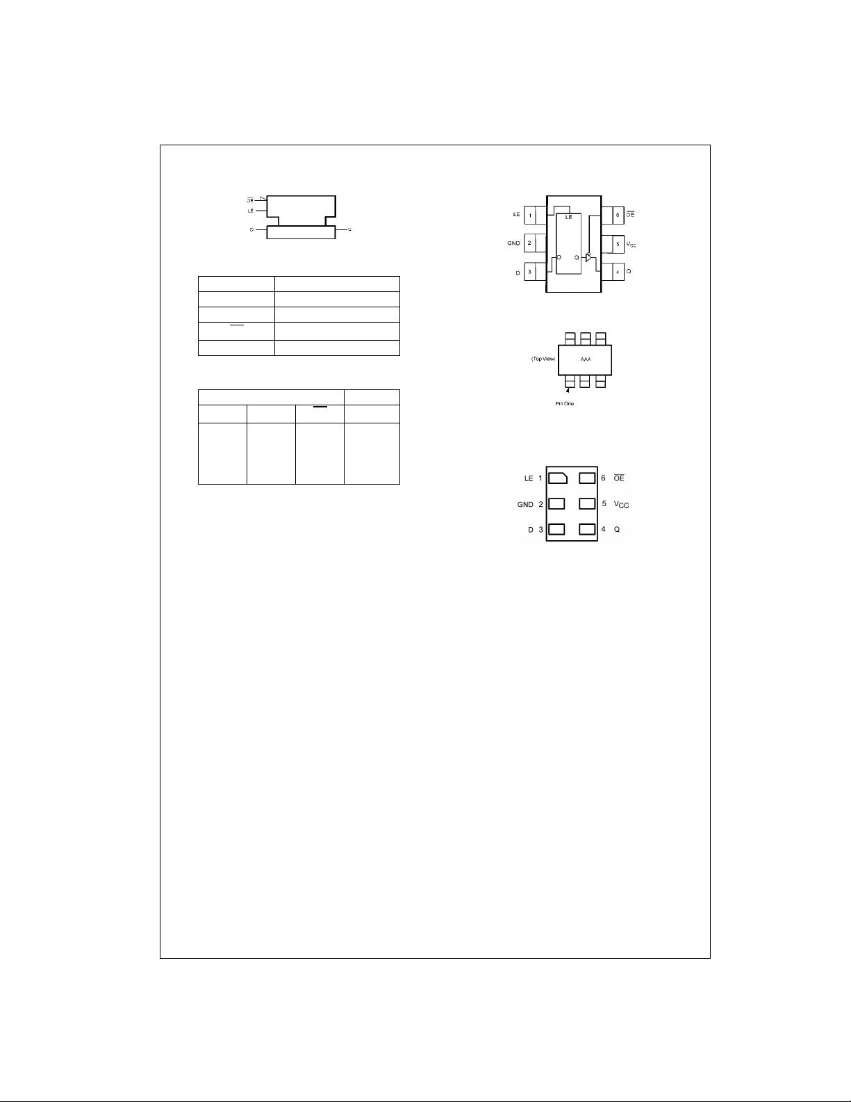
Logic Symbol
Connection Diagrams
IEEE/IEC
NC7SZ373
Pin Descriptions
Pin Names Description
D Data Input
LE Latch Enable Input
OE
Q Latch Output
Output Enable Input
Function Table
Inputs Output
LE D OE
HLL L
HHL H
LXLQ
H = HIGH Logic Level X = Immaterial
L = LOW Logic Level Z = HIGH Impedance
Q
n-1
XXH Z
= Previous state prior to HIGH-to-LOW transition of latch enable
Pin Assignments for SC70
(Top View)
Pin One Orientation Diagram
Q
n-1
AAA = Product Code Top Mark - see ordering code
Note: Orientation of Top Mark determines Pin One location. Read the top
product code mark lef t to right, Pin One is the lo w er left pin.(see diagra m ).
Pad Assignments for MicroPak
(Top Thru View)
www.fairchildsemi.com 2
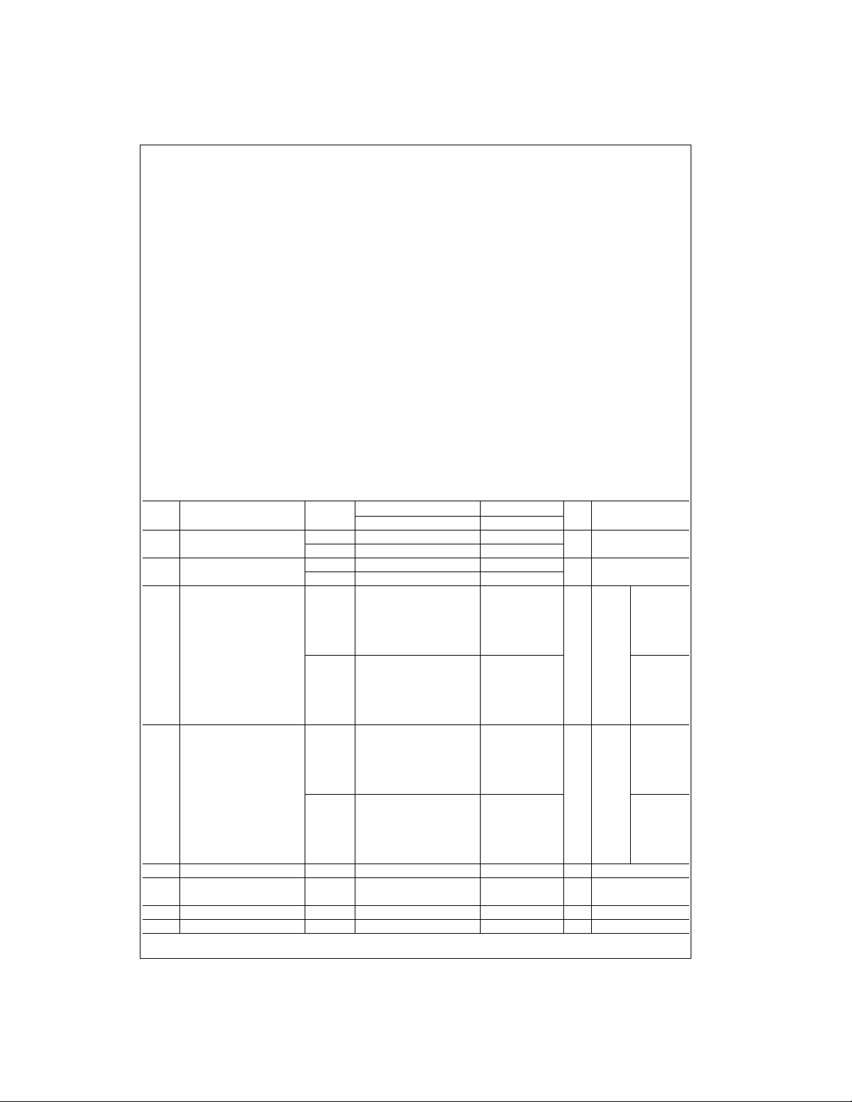
Absolute Maximum Ratings(Note 1) Recommended Operating
Supply Voltage (VCC) −0.5V to +7.0V
DC Input Voltage (V
DC Output Voltage (V
DC Input Diode Current (I
V
< 0V −50 mA
IN
DC Output Diode Current (I
< 0V −50 mA
V
OUT
DC Output (I
DC V
/GND Current (ICC/I
CC
Storage Temperature Range (T
Junction Temperature under Bias (T
Junction Lead Temperature (T
) −0.5V to +7.0V
IN
) −0.5V to +7.0V
OUT
)
IK
)
OK
) Source/Sink Current ±50 mA
OUT
) ±50 mA
GND
) −65°C to +150°C
STG
) 150°C
J
)
L
(Soldering, 10 seconds) 260
Power Dissipation (P
) @+85°C 180 mW
D
Conditions
Power Supply
Operating (V
Data Retention 1.5V to 5.5V
Input Voltage (V
Output Voltage (V
Active State 0V to V
3-STATE 0V to 5.5V
Input Rise and Fall Time (t
V
= 1.8V, 2.5V ± 0.2V 0 to 20 ns/V
CC
= 3.3V ± 0.3V 0 to 10 ns/V
V
CC
V
= 5.5V ± 0.5V 0 to 5 ns/V
°C
CC
Operating Temperature (T
Thermal Resistance (
Note 1: The “Absolute Maximum Ratings”: are those valu es b eyo nd which
the safety of the d evice cannot b e guaranteed . The device sh ould not be
operated at these limit s. The parametric values defi ned in the Electrical
Characteristics tab l es are not guar anteed at the absolute m ax imum ratings .
The “Recomm ended O peratin g Cond itions ” table will defin e the condition s
for actual device operation.
Note 2: Unused inputs must be held HIGH or LOW. They may not float.
(Note 2)
) 1.65V to 5.5V
CC
) 0V to 5.5V
IN
)
OUT
, tf)
r
) −40°C to +85°C
A
θ
) 350° C/W
JA
DC Electrical Characteristics
V
Symbol Parameter
V
HIGH Level Control 1.65 to 1.95 0.75 V
IH
Input Voltage 2.3 to 5.5 0.7 V
V
LOW Level Control 1.65 to 1.95 0.25 V
IL
Input Voltage 2.3 to 5.5 0.3 V
V
HIGH Level Control 1.65 1.55 1.65 1.55
OH
Output Voltage 1.8 1.7 1.8 1.7
V
LOW Level Control 1.65 0.0 0.08 0.0
OL
Output Voltage 1.8 0.0 0.1 0.1
I
Input Leakage Current 0 to 5.5 ±0.1 ±1.0 µA0 ≤ VIN ≤ 5.5V
IN
I
3-STATE
OZ
Output Leakage 0 ≤ V
I
Power-Off Leakage Current 0.0 1.0 10 µAVIN or V
OFF
I
Quiescent Supply Current 1.65 to 5.5 1.0 10 µAVIN = 5.5V, GND
CC
CC
(V) MinTypMaxMinMax
2.3 2.2 2.3 2.2
3.0 2.9 3.0 2.9
4.5 4.4 4.5 4.4
1.65 1.24 1.52 1.29 IOH = −4 mA
2.3 1.9 2.15 1.9 I
3.0 2.4 2.8 2.4 IOH = −16 mA
3.0 2.3 2.68 2.3 IOH = −24 mA
4.5 3.8 4.2 3.8 IOH = −32 mA
2.3 0.0 0.1 0.1
3.0 0.0 0.1 0.1
4.5 0.0 0.1 0.1
1.65 0.08 0.24 0.24 IOL = 4 mA
2.3 0.10 0.3 0.3 IOL = 8 mA
3.0 0.15 0.4 0.4 IOL = 16 mA
3.0 0.22 0.55 0.55 IOL = 24 mA
4.5 0.22 0.55 0.55 IOL = 32 mA
1.65 to 5.5 ±0.5 ±5.0 µA
TA = +25°CT
CC
CC
A
0.75 V
0.7 V
CC
CC
= −40°C to +85°C
CC
CC
0.25 V
0.3 V
CC
Unit Conditions
V
CC
V
VVIN = V
VVIN = V
IH
IL
VIN = VIL or V
≤ 5.5V
OUT
OUT
CC
IOH = −100 µA
= −8 mA
OH
IOL = 100 µA
IH
= 5.5V
NC7SZ373
3 www.fairchildsemi.com
 Loading...