

Fairchild Semiconductor NC7SZ18 Datasheet
NC7SZ18
NC7SZ18 TinyLogic
September 1999
Revised May 2003
TinyLogic
UHS 1-of-2 Non-Inverting Demultiplexer
with 3-STATE Deselected Output
General Description
The NC7SZ18 is a 1-of- 2 non-invert ing demultipl exer. The
device will buffer the data on the A pin and pass to either
output Y
or Y1 dependent on whethe r state of the select
0
pin (S) is LOW or HIGH respecti vely. The deselected output will be placed into a high impedance state. The device
is fabricated with a dvanced CMOS technolo gy to achieve
ultra high speed with high outpu t drive while maintaining
low static power dissipati on over a broad V
range. The device is s pecified to operate over the 1.6 5V to
5.5V V
operating range. The inputs and outputs are high
CC
impedance when V
5.5V independent of V
is 0V. Inputs tolerate voltages up to
CC
operating range.
CC
operating
CC
Ordering Code:
Order Package Product Code
Number Number Top Mark
NC7SZ18P6X MAA06A Z18 6-Lead SC70, EIAJ SC88, 1.25mm Wide 3k Units on Tape and Reel
NC7SZ18L6X MAC06A D5 6-Lead MicroPak, 1.0mm Wide 5k Units on Tape and Reel
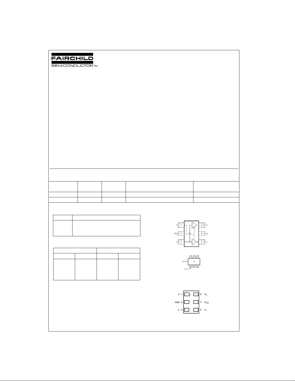
Pin Descriptions
Pin Names Description
A Data Input
S Demultiplexer Select
Y
, Y
0
1
Outputs
Features
■ Space saving SC70 6-lead surface mount package
■ Ultra small MicroPak
■ High Impedance output when deselec ted
■ Ultra High Speed: t
■ Broad VCC Operating Range; 1.65V to 5.5V
■ Power down high impedance inputs/outputs
■ Overvoltage tolerant inputs facilitate 5V to 3V translation
■ Patented noise/EMI reduction circuitry implemented
Package Descript ion Supplied As
leadless package
2.5 ns Typ into 50 pF at 5V V
PD
Connection Diagrams
Pin Assignments for SC 70
CC
UHS 1-of-2 Non-Inverting Demultiplexer with 3-STATE Deselected Output
Function Table
Input Output
SA
LLLZ
LHHZ
HLZL
HHZH
H = HIGH Logic Le v el
L = LOW Logic Level
Z = 3-STATE
TinyLogic is a registered tradema rk of Fairchild Semico nductor Corporati on.
MicroPak is a tradem ark of Fairchild Semiconductor Corporation.
© 2003 Fairchild Semiconductor Corporation DS500322 www.fairchildsemi.com
Y
0
Y
1
AAA = Product Code Top Mark - see ordering code
Note: Orientation of Top Mark determines Pin One location. Read the top
product code mark lef t to right, Pin One is the lower left pin (see diagram ).
Pin One Orientation Diagram
Pad Assignments for MicroPak
(Top Thru View)
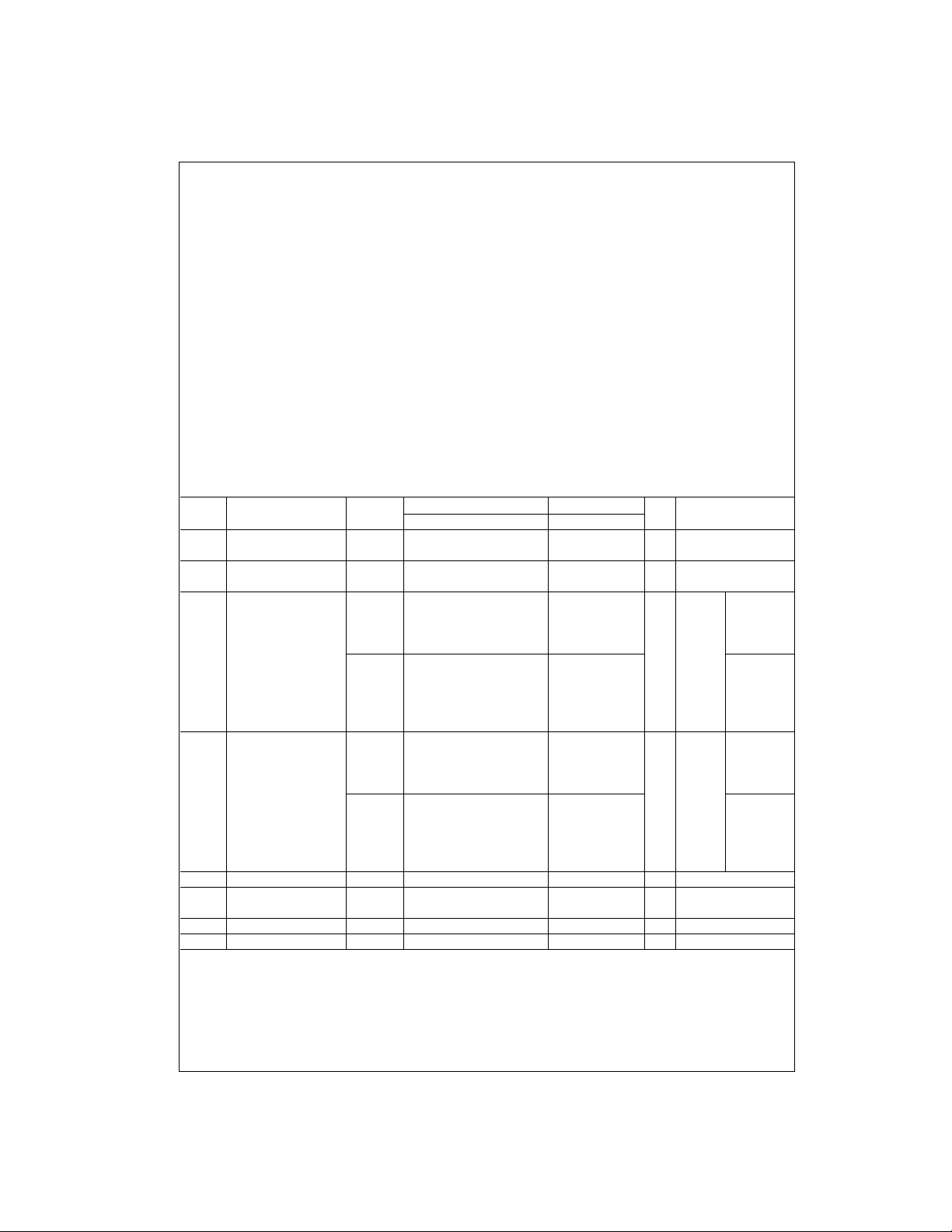
Absolute Maximum Ratings(Note 1) Recommended Operating
Supply Voltage (VCC) −0.5V to +7.0V
DC Input Voltage (V
NC7SZ18
DC Output Voltage (V
DC Input Diode Current (I
@ V
≤ −0.5V −50 mA
IN
DC Output Diode Current (I
≤ −0.5V −50 mA
@ V
IN
DC Output Current (I
DC V
or Ground Current (ICC/I
CC
Storage Temperature Range (T
Junction Temperature under Bias (T
Junction Lead Temperature (T
) −0.5V to +7.0V
IN
) −0.5V to +7.0V
OUT
)
IK
)
OK
) ±50 mA
OUT
) ±100 mA
GND
) −65°C to +150°C
STG
) 150°C
J
)
L
(Soldering, 10 seconds) 260
Power Dissipation (P
) @ +85°C 180 mW
D
Conditions
Supply Voltage Operating (V
Supply Voltage Data Retention (V
Input Voltage (V
Output Voltage (V
)0V to 5.5V
IN
OUT
Operating Temperature (TA) −40°C to +85°C
Input Rise and Fall Time (t
@ 1.8V ± 0.15V, 2.5V ± 0.2V 0 ns/V to 20 ns/V
V
CC
V
@ 3.3V ± 0.3V 0 ns/V to 10 ns/V
CC
V
@ 5.0V ± 0.5V 0 ns/V to 5 ns/V
CC
Thermal Resistance (
Note 1: Absolute maximum ratings are DC values beyond which the devi ce
may be damage d or h ave its us eful life im pai red. Th e dat as heet sp ecific a-
°C
tions should be met, without exception, to ensure that the system design is
reliable over its power supply, temperature, and output/input loading variables. Fairchild does no t recommend operation outsid e datasheet spec ifications.
) 1.65V to 5.5V
CC
) 0V to V
, tf)
r
θ
)350°C/W
JA
DC Electrical Characteristics
V
Symbol Parameter
V
HIGH Level 1.65 − 1.95 0.75 V
IH
Input Voltage 2.3 − 5.5 0.7 V
V
LOW Level 1.65 − 1.95 0.25 V
IL
Input Voltage 2.3 − 5.5 0.3 V
V
HIGH Level 1.65 1.55 1.65 1.55
OH
Output Voltage 2.3 2.2 2.3 2.2
LOW Level 1.65 0.0 0.10 0.10
V
OL
Output Voltage 2.3 0.0 0.10 0.10
I
Input Leakage Current 0 to 5.5 ±0.1 ±1 µAVIN = 5.5V, GND
IN
I
3-STATE Output Leakage 1.65 to 5.5V ±0.5 ±5 µAVIN = VIL or V
OZ
I
Power Off Leakage Current 0.0 1 10 µAVIN or V
OFF
I
Quiescent Supply Current 1.8 to 5.5 1 10 µAVIN = 5.5V, GND
CC
CC
(V) MinTypMaxMinMax
3.0 2.9 3.0 2.9
4.5 4.4 4.5 4.4
1.65 1.29 1.52 1.29 IOH = −4 mA
2.3 1.9 2.15 1.9 I
3.0 2.4 2.80 2.4 I
3.0 2.3 3.68 2.3 IOH = −24 mA
4.5 3.8 4.20 3.8 I
3.0 0.0 0.10 0.10
4.5 0.0 0.10 0.10
1.65 0.08 0.24 0.24 IOL = 4 mA
2.3 0.10 0.3 0.3 IOL = 8 mA
3.0 0.15 0.4 0.4 IOL = 16 mA
3.0 0.22 0.55 0.55 IOL = 24 mA
4.5 0.22 0.55 0.55 IOL = 32 mA
TA = +25°CT
CC
CC
A
0.75 V
0.7 V
CC
CC
= −40°C to +85°C
CC
CC
0.25 V
0.3 V
CC
Units Conditions
CC
) 1.5V to 5.5V
CC
V
V
IOH = −100 µA
VVIN = V
VVIN = V
0 < V
IH
IL
OUT
OUT
OH
OH
OH
IOL = 100 µA
IH
≤ 5.5V
= 5.5V
CC
= −8 mA
= −16 mA
= −32 mA
www.fairchildsemi.com 2
AC Electrical Characteristics
V
Symbol Parameter
t
Propagation Delay 1.8 ± 0.15 2.0 6.3 10.1 2.0 10.5
PLH
t
A to Y0 or Y
PHL
1
CC
(V) Min Typ Max Min Max Number
2.5 ± 0.2 1.0 3.6 5.7 1.0 6.0 RD = 1 MΩ
3.3 ± 0.3 0.8 2.7 4.0 0.8 4.3 S1 = OPEN
5.0 ± 0.5 0.5 2.0 3.1 0.5 3.3
t
Propagation Delay 3.3 ± 0.3 1.2 3.4 4.9 1.2 5.4
PLH
t
A to Y0 or Y
PHL
Output Enable Time 1.8 ± 0.15 3.0 6.9 12.0 3.0 12.5
t
PZL
t
PZH
1
5.0 ± 0.5 0.8 2.5 3.9 0.8 4.2 RL = 500Ω
2.5 ± 0.2 1.8 4.2 6.8 1.8 7.3 RD, RU = 500Ω
3.3 ± 0.3 1.2 3.2 5.0 1.2 5.5 S1 = GND for t
5.0 ± 0.5 0.8 2.5 4.0 0.8 4.3 S1 = VIN for t
t
Output Disable Time 1.8 ± 0.15 2.5 6.0 10.0 2.5 10.5
PLZ
t
PHZ
2.5 ± 0.2 1.5 4.0 6.8 1.5 7.1 RD, RU = 500Ω
3.3 ± 0.3 0.8 2.9 4.9 0.8 5.3 S1 = GND for t
5.0 ± 0.5 0.3 1.8 3.5 0.3 3.7 S1 = VIN for t
C
Input Capacitance OPEN 2.5
IN
C
Output Capacitance 3.3V 4.0
OUT
C
Power Dissipation 3.3 16
PD
Capacitance 5.0 19.5
Note 2: CPD is defined as the value of the internal equivalent capacitance which is derived from dynamic operating current consumption (I
loading and operating at 50% duty cycle. (See Figure 2.) C
= (CPD)(VCC)(fIN) + (ICCstatic).
I
CCD
TA = +25°CT
is related to I
PD
dynamic operating current by the express ion:
CCD
= −40°C to +85°C
A
Units Conditions
CL = 15 pF,
ns
CL = 50 pF,
ns
S1 = OPEN
CL = 50 pF
ns
VI = 2 x V
CL = 50 pF
ns
VI = 2 x V
pF
pF (Note 2) Figure 2
PZH
PZL
CC
PHZ
PLZ
CC
) at no output
CCD
Figure
Figures
1, 3
Figures
1, 3
Figures
1, 3
Figures
1, 3
NC7SZ18
3 www.fairchildsemi.com
 Loading...