

Fairchild Semiconductor MM74HCT164N, MM74HCT164SJ, MM74HCT164CW, MM74HCT164SJX, MM74HCT164M Datasheet
February 1984
Revised February 1999
MM74HCT164 8-Bit Serial-in/Parallel-out Shift Register
© 1999 Fairchild Semiconductor Corporation DS005765.prf www.fairchildsemi.com
MM74HCT164
8-Bit Serial-in/Parallel-out Shift Register
General Description
The MM74HCT164 utilizes advanced silicon-gate CMOS
technology. It has the high noise immunity and low consumption of standard CMOS integrated circuits. It also
offers speeds comparable to low power Schottky devices.
This 8-bit shift register has ga ted ser ia l inp uts a nd CLE AR.
Each register bit is a D-type master/slave flip-flop. Inputs A
& B permit complete control over the incoming data. A
LOW at either or both inputs inhibits entr y of new data and
resets the first flip-flop to the low level at the next clock
pulse. A HIGH level on one input enables the o ther input
which will then determine the state of the first flip-flop. Data
at the serial inputs may be changed while the clock is HIGH
or LOW, but only information meeting the setup and hold
time requirements will be entered. Data is serially shifted in
and out of the 8-bit register during the positive going transition of the clock pulse. Cle ar is independent of t he clock
and accomplished by a low level at the CLEAR input.
The 74HCT logic family is f unctionally as well as pin-ou t
compatible with the standard 74LS logic family. All inputs
are protected from damage due to static discharge by internal diode clamps to V
CC
and ground.
MM74HCT devices are intended to interface between TTL
and NMOS components and standard CMOS devices.
These parts are also plug-in replacements for LS-TTL
devices and can be used to redu ce power consumption in
existing designs.
Features
■ Typical propagation delay: 20 ns
■ Low quiescent current: 40 µA maximum (74HCT Series)
■ Low input current: 1 µA maximum
■ Fanout of 10 LS-TTL loads
■ TTL input compatible
Ordering Code:
Devices also available in Tape and Reel. Specify by appending the suffix letter “X” to t he ordering code.
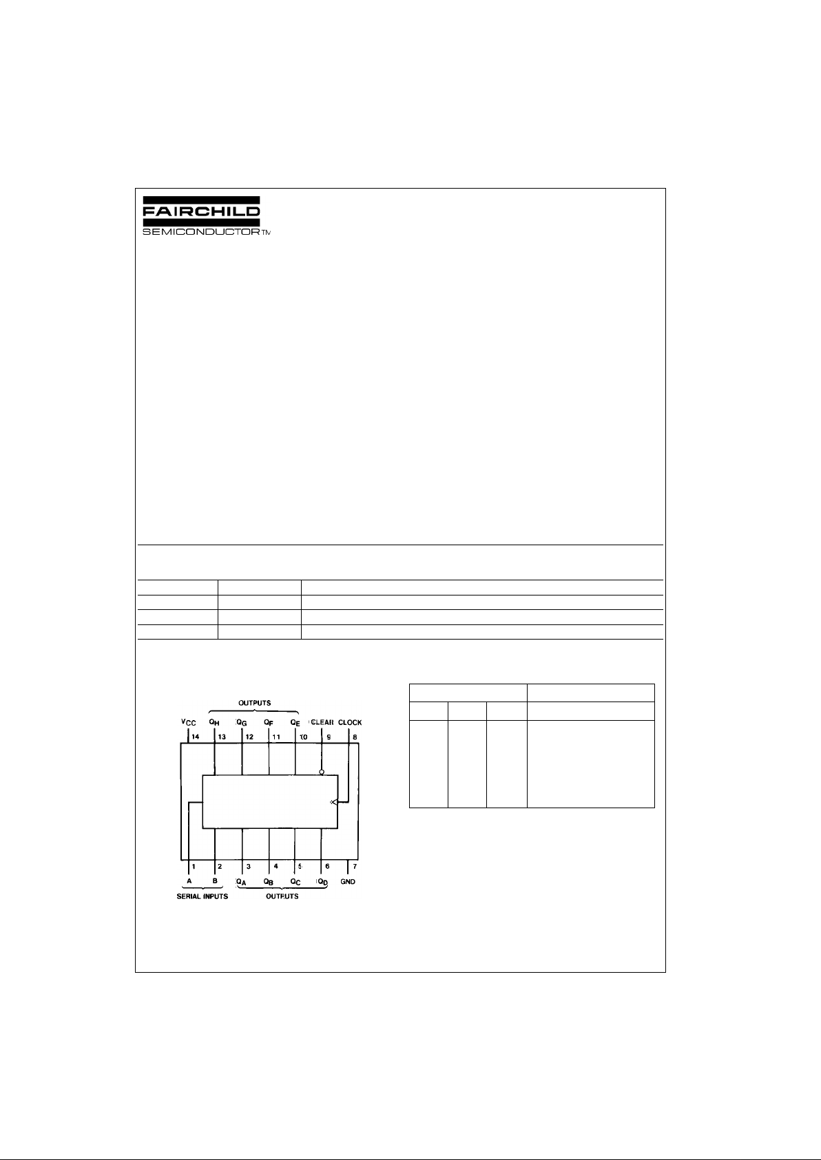
Connection Diagram
Pin Assignments for DIP, SOIC and SOP
Top View
Truth Table
H = HIGH Level (steady state)
L = LOW Level (steady state)
X = Irrelevant (any input, including trans iti ons)
↑ = Transition from LOW-to-HIGH level.
Q
AO
, QBO, QHO = the level of QA, QB, or QH, respectively, before the
indicated steady state input conditions were established.
Q
An
, QGn = The level of QA or QG before the most recent ↑ transition of
the clock; indicated a one-bit shift.
Order Number Package Number Package Description
MM74HCT164M M14A 14-Lead Small Outline Integrated Circuit (SOIC), JEDEC MS-120, 0.150” Narrow
MM74HCT164SJ M14D 14-Lead Small Outline Package (SOP), EIAJ TYPE II, 5.3mm Wide
MM74HCT164N N14A 14-Lead Plastic Dual-In-Line Package (PDIP) JEDEC MS-001, 0.300” Wide
Inputs Outputs
Clear Clock A B Q
AQB
... Q
H
LXXXLL L
HLXXQ
AOQBO
Q
HO
H ↑ HH H Q
An
Q
Gn
H ↑ LX L Q
An
Q
Gn
H ↑ XL L Q
An
Q
Gn
www.fairchildsemi.com 2
MM74HCT164
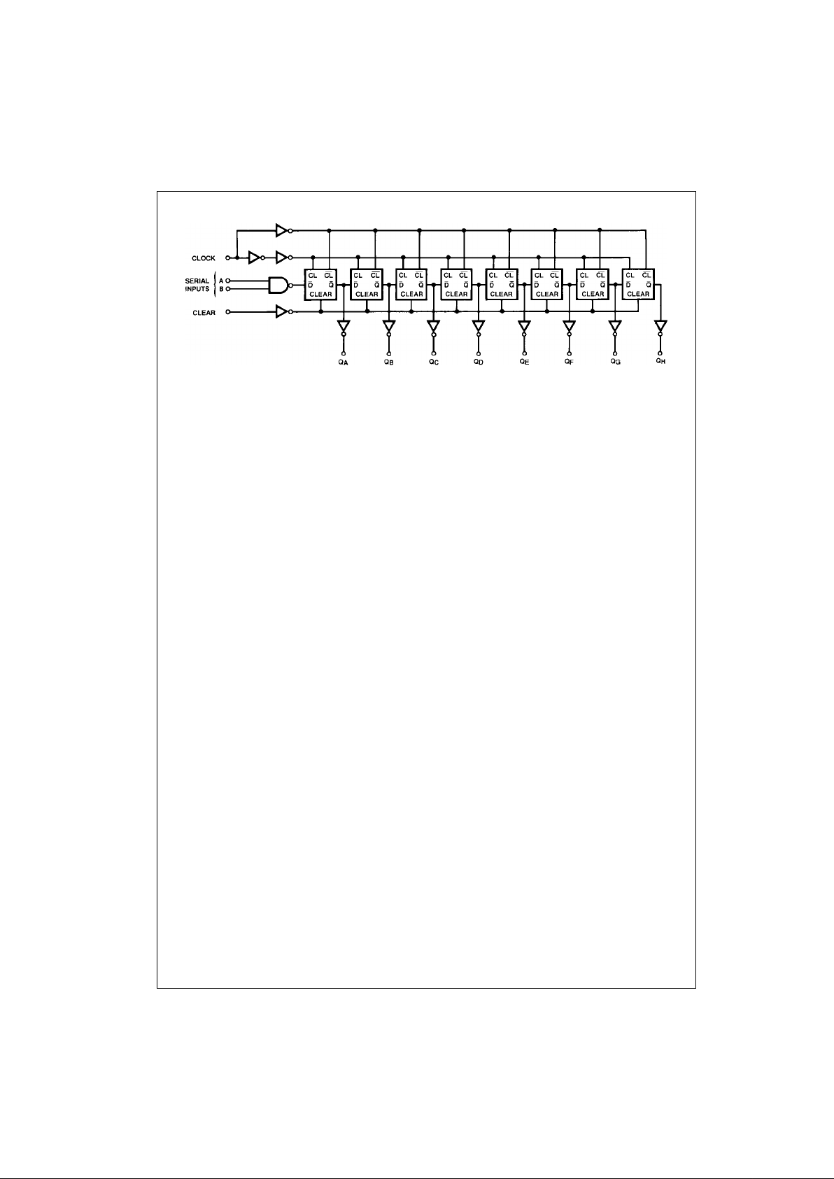
Logic Diagram
 Loading...