Fairchild Semiconductor MM74HCT14SJ, MM74HCT14MX, MM74HCT14MTC, MM74HCT14M, MM74HCT14SJX Datasheet
...
September 1983
Revised April 1999
MM74HCT14 Hex Inverting Schmitt Trigger
© 1999 Fairchild Semiconductor Corporation DS500059.prf www.fairchildsemi.com
MM74HCT14
Hex Inverting Schmitt Trigger
General Description
The MM74HCT14 utilizes advanced silicon-gate CMOS
technology to achieve the low power dissipation and high
noise immunity of standard CMOS, as well as the capability
to drive 10 L S-TTL loads.
The 74HCT logic family is function ally and pinout compa tible with the standard 74L S logic family. All inputs are pr otected from damage due to static discharge by internal
diode clamps to V
CC
and ground.
Features
■ Typical propagation delay: 13 ns
■ Wide power supply range: 2–6V
■ Low quiescent current: 10 µA maximum
■ Low input current: 1 µA maximum
■ Fanout of 10 LS-TTL loads
■ Typical hysteresis voltage: 0.9V at V
CC
= 4.5V
■ TTL, LS pin-out and input threshold compatible
Ordering Codes:
Devices also availab le in Tape and Reel. Specify by appending th e s uffix let t er “X” to the ordering cod e.
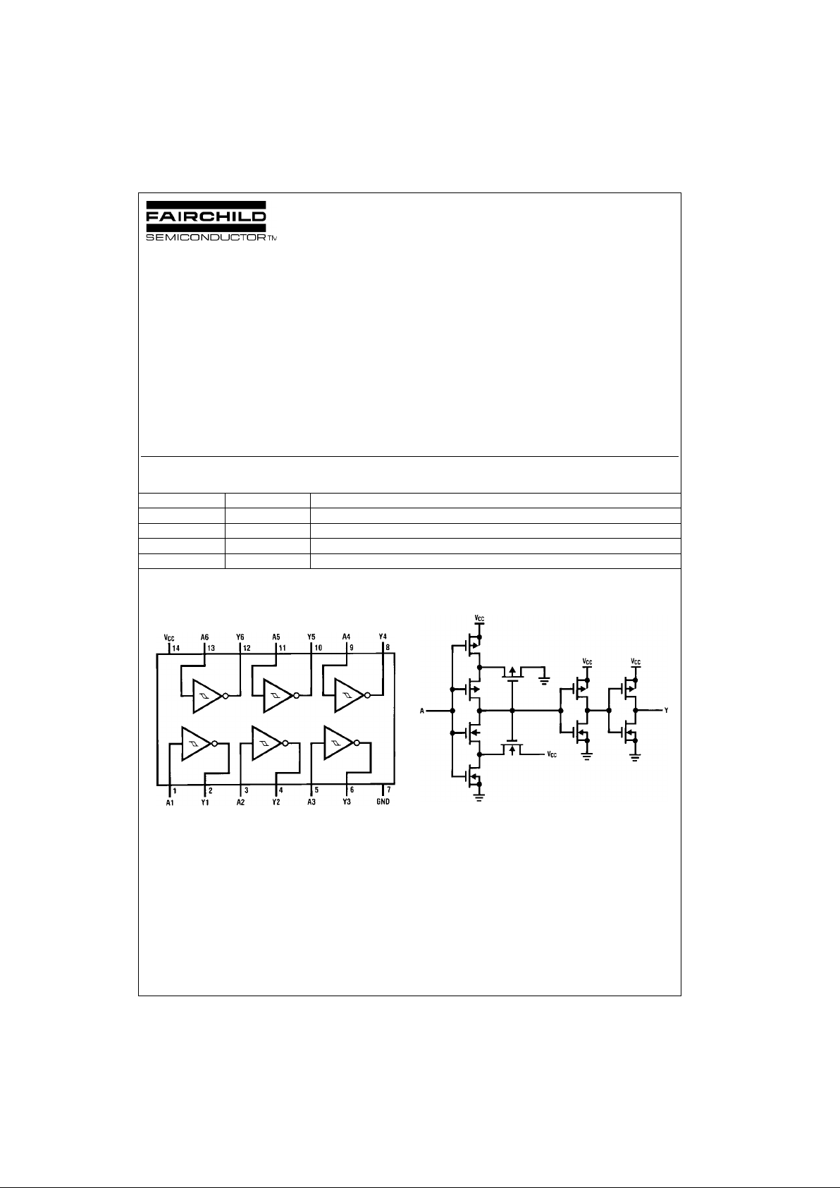
Connection Diagram
Pin Assignments f or DIP, SOIC, SOP and TSSOP
Top View
Schematic Diagram
Order Number Package Number Package Description
MM74HCT14M M14A 14-Lead Small Outline Integrated Circuit (SOIC), JEDEC MS-120, 0.150” Narrow
MM74HCT14SJ M14D 14-Lead Small Outline Package (SOP), EIAJ TYPE II, 5.3mm Wide
MM74HCT14MTC MTC14 14-Lead Thin Shrink Small Outline Package (TSSOP), JEDEC MO-153, 4.4mm Wide
MM74HCT14N N14A 14-Lead Plastic Dual-In-Line Package (PDIP), JEDEC MS-001, 0.300” Wide

www.fairchildsemi.com 2
MM74HCT14
Absolute Maximum Ratings(Note 1)
(Note 2)
Recommended Operating
Conditions
Note 1: Absolute Maximum Ratings are those values beyond which dam-
age to the device may occur.
Note 2: Unless otherwise specified all voltages are referenced to ground.
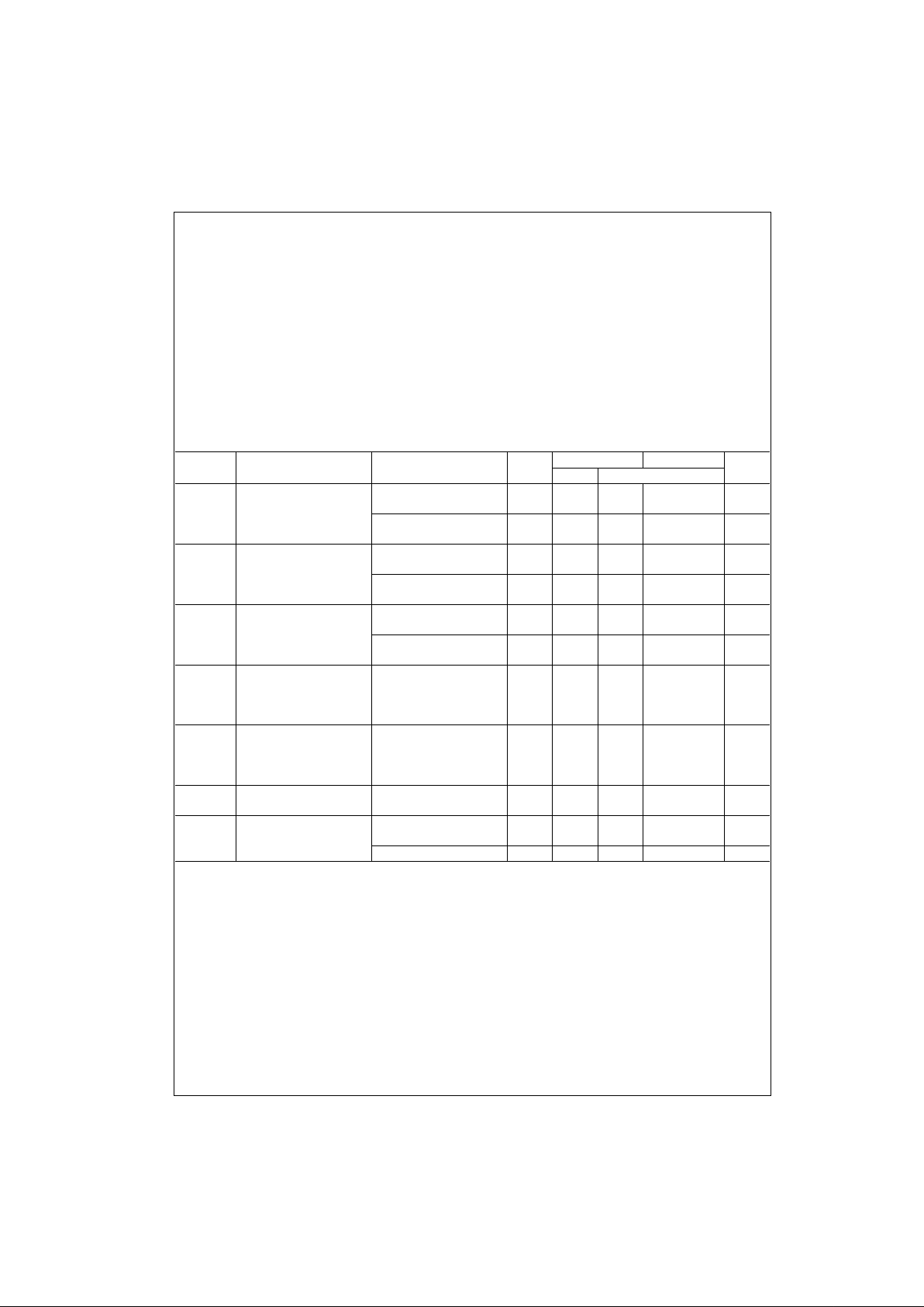
DC Electrical Characteristics (Note 3)
Note 3: For a power suppl y of 5V ± 10% t he worst cas e outpu t voltages (VOH, and VOL) occur for HC at 4.5V. Thus the 4.5V values shou ld be used when
designing with this supply. Worst case V
IH
and VIL occur at VCC = 5.5V and 4.5V respectively. (The VIH value at 5.5V is 3.85V.) The worst case leakage cur-
rent (I
IN
, ICC, and IOZ) occur for CMOS at the higher voltage and so th e 6. 0V values should be us ed.
Supply Voltage (VCC) −0.5 to +7.0V
DC Input Voltage (V
IN
) −1.5 to V
CC
+ 1.5V
DC Output Voltage (V
OUT
) −0.5 to V
CC
+ 0.5V
Clamp Diode Current (I
IK
, IOK) ± 20 mA
DC Output Current, per pin (I
OUT
) ± 25 mA
DC V
CC
or GND Current, per pin (ICC) ± 50 mA
Storage Temperature Range (T
STG
) −65°C to +150°C
Lead Temperature (T
L
)
(Soldering 10 seconds) 260°C
Min Max Units
Supply Voltage (V
CC
)26V
DC Input or Output Voltage
(V
IN
, V
OUT
)0V
CC
V
Operating Temperature Range (T
A
) −40 +85 °C
Symbol Parameter Conditions
V
CC
TA = 25°CTA = −40 to 85°C
Units
Typ Guaranteed Limits
V
T+
Positive Going Minimum 4.5V 1.5 1.2 1.2 V
Threshold Voltage 5.5V 1.7 1.4 1.4 V
Maximum 4.5V 1.5 1.9 1.9 V
5.5V 1.7 2.1 2.1 V
V
T−
Negative Going Minimum 4.5V 0.9 0.5 0.5 V
Threshold Voltage 5.5V 1.0 0.6 0.6 V
Maximum 4.5V 0.9 1.2 1.2 V
5.5V 1.0 1.4 1.4 V
V
H
Hysteresis Voltage Minimum 4.5V 0.6 0.4 0.4 V
5.5V 0.7 0.4 0.4 V
Maximum 4.5V 0.6 1.4 1.4 V
5.5V 0.7 1.5 1.5 V
V
OH
Minimum HIGH Level VIN = V
IL
Output Voltage |I
OUT
| = 20 µAV
CCVCC
− 0.1 VCC − 0.1 V
|I
OUT
| = 4.0 mA, VCC = 4.5V 4.2 3.98 3.84 V
|I
OUT
| = 4.8 mA, VCC = 5.5V 5.2 4.98 4.98 V
V
OL
Maximum LOW Level VIN = V
IH
Voltage |I
OUT
| = 20 µA00.10.1V
|I
OUT
| = 4.0 mA, VCC = 4.5V 0.2 0.26 0.33 V
|I
OUT
| = 4.8 mA, VCC = 5.5V 0.2 0.26 0.33 V
I
IN
Maximum Input Current VIN = VCC or GND
±0.1 ±1.0 µA
VIH or V
IL
I
CC
Maximum Quiescent VIN = VCC or GND
5.5V 1.0 10 µA
Supply Current I
OUT
= 0 µA
VIN=2.4V or 0.5V (Note 3) 5.5V 2.4 2.4 mA
 Loading...