

Fairchild Semiconductor ML4803CP1 Datasheet
January 2001
PRELIMINARY
ML4803
8-Pin PFC and PWM Controller Combo
GENERAL DESCRIPTION
The ML4803 is a space-saving controller for power factor
corrected, switched mode power supplies that offers very
low start-up and operating currents.
Power Factor Correction (PFC) offers the use of smaller,
lower cost bulk capacitors, reduces power line loading
and stress on the switching FETs, and results in a power
supply fully compliant to IEC1000-3-2 specifications. The
ML4803 includes circuits for the implementation of a
leading edge, average current “boost” type PFC and a
trailing edge, PWM.
The ML4803-1’s PFC and PWM operate at the same
frequency, 67kHz. The PFC frequency of the ML4803-2 is
automatically set at half that of the 134kHz PWM. This
higher frequency allows the user to design with smaller
PWM components while maintaining the optimum
operating frequency for the PFC. An overvoltage
comparator shuts down the PFC section in the event of a
sudden decrease in load. The PFC section also includes
peak current limiting for enhanced system reliability.
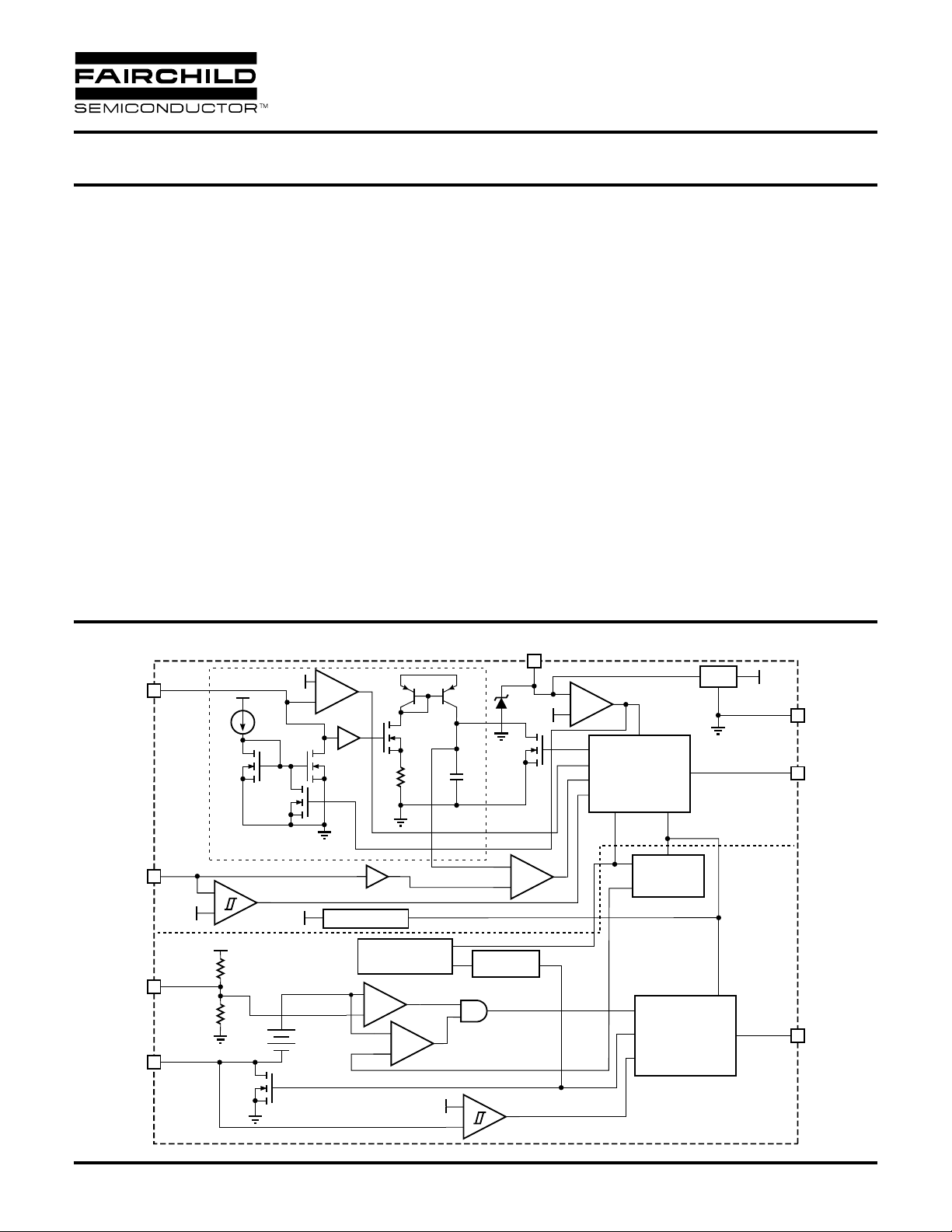
BLOCK DIAGRAM
4
3
5
6
VEAO
I
SENSE
–1V
V
DC
I
LIMIT
35µA
M1
M7
ONE PIN ERROR AMPLIFIER
PFC I
LIMIT
V
M6
26k
40k
+
–
V
REF
7V
CC
+
COMP
–
–1
M2
PFC/PWM UVLO
1.2V
PFC OFF
–4
PWM – 134kHz
–
COMP
+
M3
R1 C1
OSCILLATOR
PFC – 67kHz
PWM COMPARATOR
–
COMP
+
1.5V
FEATURES
■ Internally synchronized PFC and PWM in one 8-pin IC
■ Patented one-pin voltage error amplifier with advanced
input current shaping technique
■ Peak or average current, continuous boost, leading
edge PFC (Input Current Shaping Technology)
■ High efficiency trailing-edge current mode PWM
■ Low supply currents; start-up: 150µA typ., operating:
2mA typ.
■ Synchronized leading and trailing edge modulation
■ Reduces ripple current in the storage capacitor
between the PFC and PWM sections
■ Overvoltage, UVLO, and brownout protection
■ PFC V
30pF
DUTY CYCLE
LIMIT
DC I
–
+
V
CC
17.5V
M4
+
COMP
–
LIMIT
OVP with PFC Soft Start
CC
7
VCC OVP
+
COMP
16.2V
–
CONTROL
PFC
LOGIC
SOFT START
PWM
CONTROL
LOGIC
REF
V
REF
GND
PFC OUT
LEADING
EDGE PFC
TRAILING
EDGE PWM
PWM OUT
2
1
8
REV. 1.1 1/24/2001
ML4803
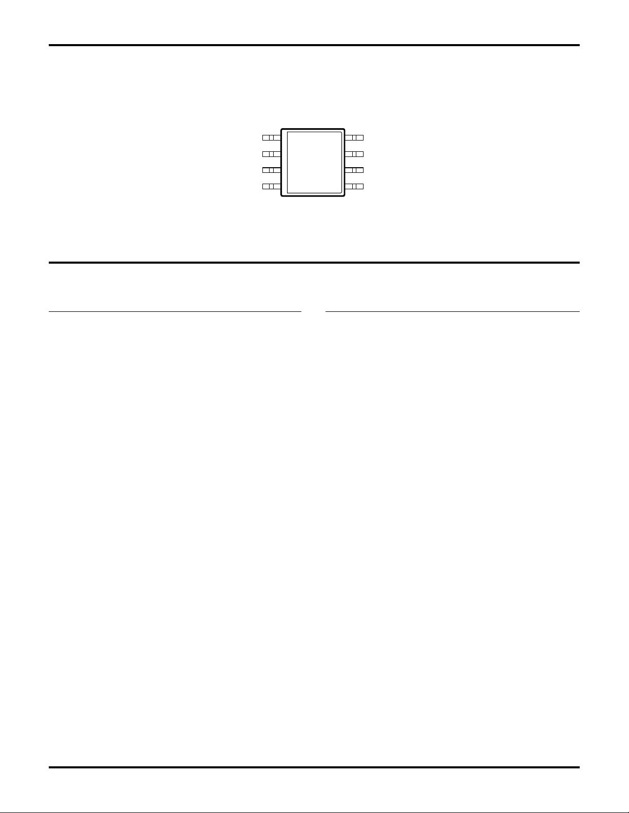
PIN CONFIGURATION
PIN DESCRIPTION
PFC OUT
GND
I
SENSE
VEAO
ML4803
8-Pin PDIP (P08)
8-Pin SOIC (S08)
1
2
3
4
TOP VIEW
8
7
6
5
PWM OUT
V
CC
I
LIMIT
V
DC
PIN NAME FUNCTION
1 PFC OUT PFC driver output
2 GND Ground
3I
SENSE
Current sense input to the PFC current
limit comparator
4 VEAO PFC one-pin error amplifier input
PIN NAME FUNCTION
5V
DC
6I
LIMIT
7V
CC
PWM voltage feedback input
PWM current limit comparator input
Positive supply (may require an
external shunt regulator)
8 PWM OUT PWM driver output
2 REV. 1.1 1/24/2001
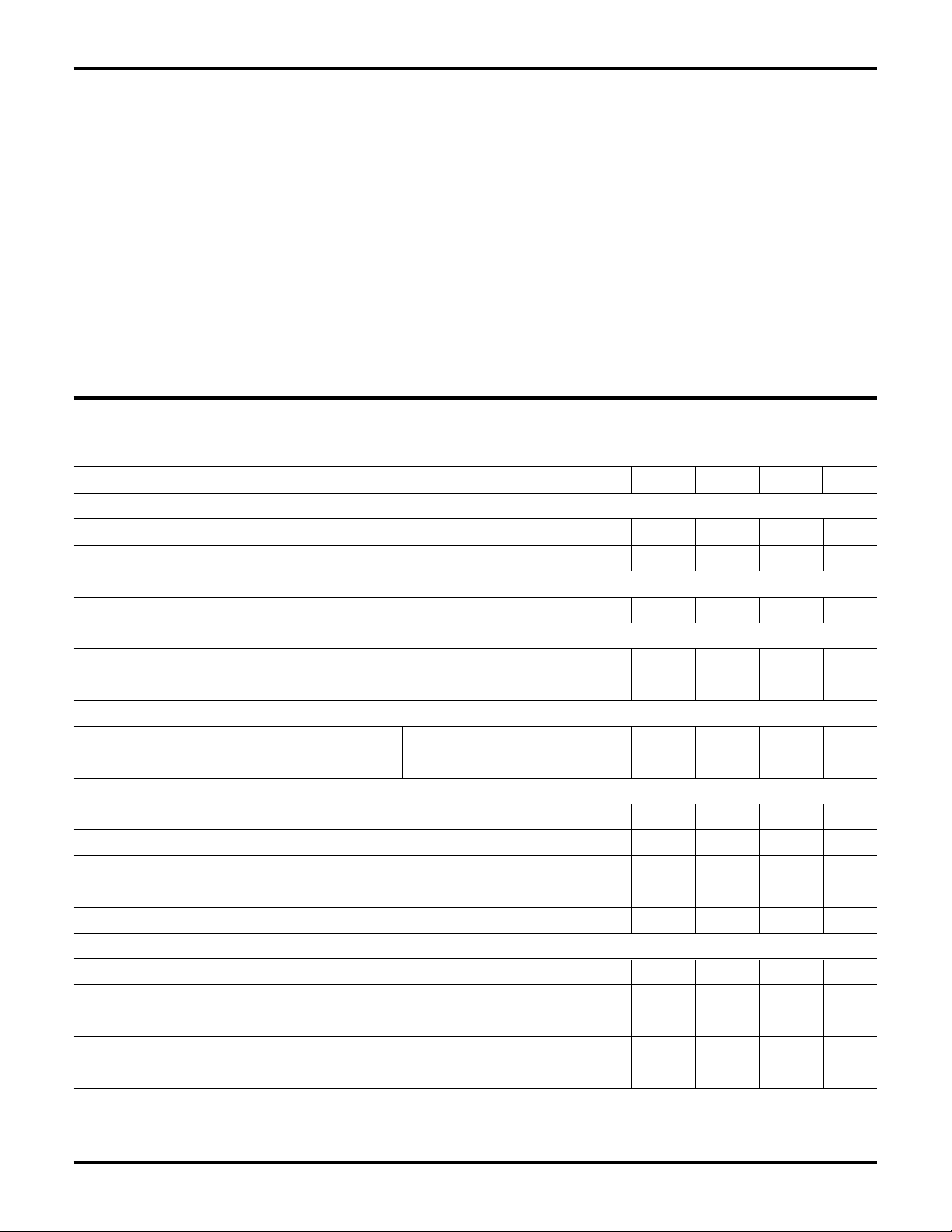
ABSOLUTE MAXIMUM RATINGS
ML4803
Absolute maximum ratings are those values beyond which
the device could be permanently damaged. Absolute
maximum ratings are stress ratings only and functional
device operation is not implied.
Junction Temperature ............................................. 150°C
Storage Temperature Range...................... –65°C to 150°C
Lead Temperature (Soldering, 10 sec)..................... 260°C
Thermal Resistance (θ
)
JA
Plastic DIP ..................................................... 110°C/W
I
Current (average) ..............................................40mA
CC
MAX ................................................................18.3V
V
CC
I
Voltage .................................................. -5V to 1V
SENSE
Voltage on Any Other Pin ...... GND - 0.3V to V
CC
+ 0.3V
Plastic SOIC ................................................... 160°C/W
OPERATING CONDITIONS
Peak PFC OUT Current, Source or Sink ....................... 1A
Peak PWM OUT Current, Source or Sink..................... 1A
PFC OUT, PWM OUT Energy Per Cycle................... 1.5µJ
Temperature Range
ML4803CX-X ............................................. 0°C to 70°C
ML4803IX-X ........................................... -40°C to 85°C
ELECTRICAL CHARACTERISTICS
Unless otherwise specified, VCC = 15V, TA = Operating Temperature Range (Note 1)
SYMBOL PARAMETER CONDITIONS MIN TYP MAX UNITS
ONE-PIN ERROR AMPLIFIER
VEAO Output Current TA = 25ºC, V
Line Regulation 10V < VCC < 15V, V
VCC OVP COMPARATOR
Threshold Voltage TA = 0ºC to 70ºC 15.5 16.0 16.5 V
PFC I
DC I
OSCILLATOR
PFC
COMPARATOR
LIMIT
Threshold Voltage -0.9 -1 -1.15 V
Delay to Output 150 300 ns
COMPARATOR
LIMIT
Threshold Voltage 1.4 1.5 1.6 V
Delay to Output 150 300 ns
Initial Accuracy TA = 25°C 626774kHz
Voltage Stability 10V < VCC < 15V 1 %
Temperature Stability 2%
Total Variation Over Line and Temp 60 67 74.5 kHz
Dead Time PFC Only 0.3 0.45 0.65 µs
Minimum Duty Cycle V
Maximum Duty Cycle V
Output Low Impedance 8 15 Ω
EAO
EAO
> 7.0V,I
< 4.0V,I
= 6V 33.5 35.0 36.5 µA
EAO
= 6V 0.1 0.3 µA
EAO
= -0.2V 0 %
SENSE
= 0V 90 95 %
SENSE
Output Low Voltage I
REV. 1.1 1/24/2001 3
= -100mA 0.8 1.5 V
OUT
I
= –10mA, VCC = 8V 0.7 1.5 V
OUT
ML4803
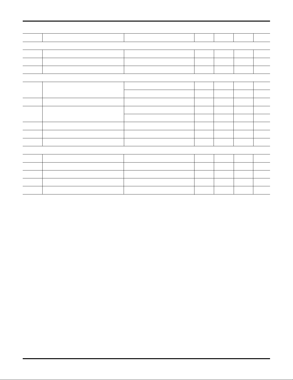
ELECTRICAL CHARACTERISTICS (Continued)
SYMBOL PARAMETER CONDITIONS MIN TYP MAX UNITS
PFC (Continued)
Output High Impedance 8 15 Ω
Output High Voltage I
Rise/Fall Time CL = 1000pF 50 ns
PWM
Duty Cycle Range TA = 0ºC to 70ºC, ML4803-2 0-43 0-47 0-50 %
Output Low Impedance 8 15 Ω
Output Low Voltage I
Output High Impedance 8 15 Ω
= 100mA, VCC = 15V 13.5 14.2 V
OUT
TA = 0ºC to 70ºC, ML4803-1 0-49.5 0-50 %
= –100mA 0.8 1.5 V
OUT
I
= –10mA, VCC = 8V 0.7 1.5 V
OUT
Output High Voltage I
Rise/Fall Time CL = 1000pF 50 ns
SUPPLY
VCC Clamp Voltage (V
Start-up Current VCC = 11V, CL = 0 0.2 0.4 mA
Operating Current VCC = 15V, CL = 0 2.5 4 mA
Undervoltage Lockout Threshold 11.5 12 12.5 V
Undervoltage Lockout Hysteresis 2.4 2.9 3.4 V
Note 1: Limits are guaranteed by 100% testing, sampling, or correlation with worst case test conditions.
)I
CCZ
= 100mA, VCC = 15V 13.5 14.2 V
OUT
= 10mA 16.7 17.5 18.3 V
CC
4 REV. 1.1 1/24/2001
 Loading...