

Fairchild Semiconductor ML4800CP Datasheet
March 2001
PRELIMINARY
ML4800
Power Factor Correction and PWM Controller Combo
GENERAL DESCRIPTION
The ML4800 is a controller for power factor corrected,
switched mode power supplies. Power Factor Correction
(PFC) allows the use of smaller, lower cost bulk capacitors,
reduces power line loading and stress on the switching
FETs, and results in a power supply that fully complies
with IEC1000-3-2 specification. Intended as a BiCMOS
version of the industry-standard ML4824, the ML4800
includes circuits for the implementation of leading edge,
average current, “boost” type power factor correction and
a trailing edge, pulse width modulator (PWM). It also
includes a TriFault Detect™ function to help ensure that no
unsafe conditions will result from single component failure
in the PFC. Gate-drivers with 1A capabilities minimize the
need for external driver circuits. Low power requirements
improve efficiency and reduce component costs.
An over-voltage comparator shuts down the PFC section in
the event of a sudden decrease in load. The PFC section
also includes peak current limiting and input voltage
brownout protection. The PWM section can be operated in
current or voltage mode, at up to 250kHz, and includes an
accurate 50% duty cycle limit to prevent transformer
saturation.
FEATURES
■ Internally synchronized leading-edge PFC and trailing-
edge PWM in one IC
■ TriFault Detect™ for UL1950 compliance and
enhanced safety
■ Slew rate enhanced transconductance error amplifier
for ultra-fast PFC response
■ Low power: 200µA startup current, 5.5mA operating
current
■ Low total harmonic distortion, high PF
■ Reduced ripple current in storage capacitor between
PFC and PWM sections
■ Average current, continuous boost leading edge PFC
■ PWM configurable for current-mode or voltage mode
operation
■ Current fed gain modulator for improved noise immunity
■ Overvoltage and brown-out protection, UVLO, and soft
start
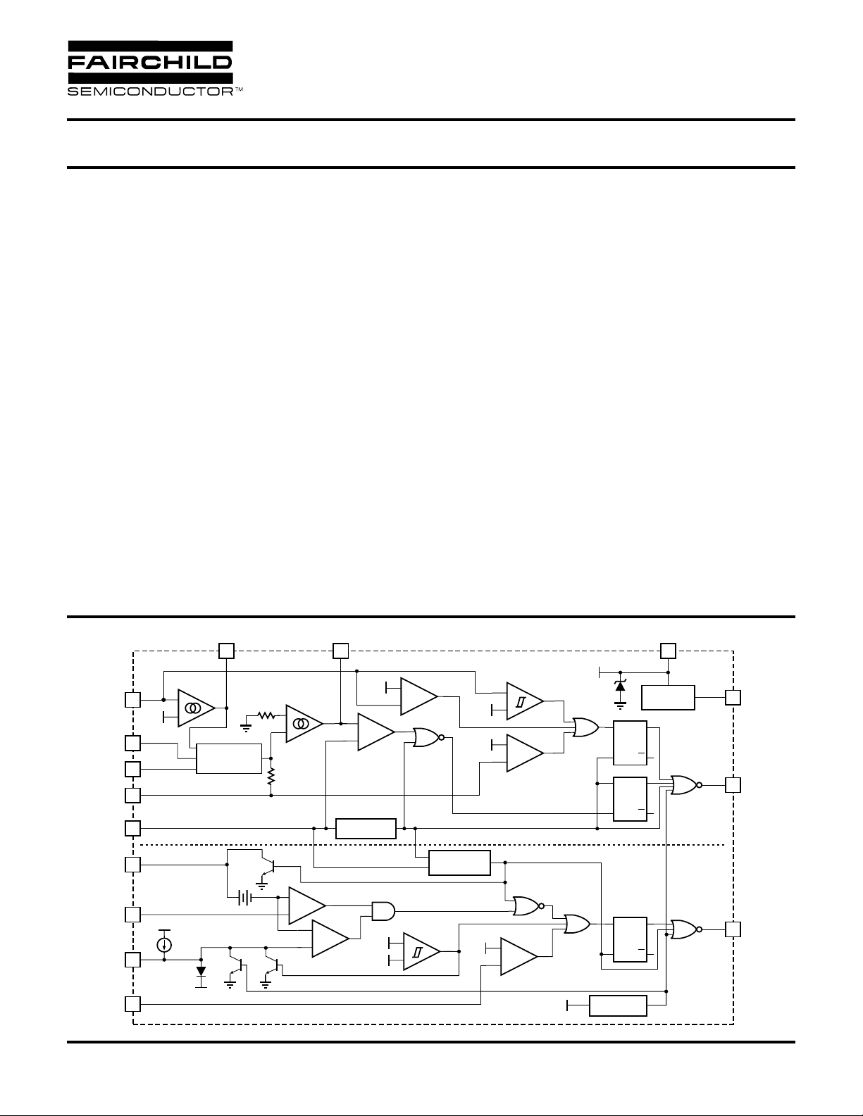
BLOCK DIAGRAM
VEAO
15
2
4
3
7
8
6
5
9
V
2.5V
I
AC
V
I
SENSE
RAMP 1
RAMP 2
V
SS
DC I
FB
RMS
DC
V
CC
LIMIT
VEA
-
+
25µA
MODULATOR
1.25V
V
REF
16
GAIN
1.6kΩ
1.6kΩ
1
IEAO
IEA
+
-
-
+
-
+
POWER FACTOR CORRECTOR
0.5V
+
-
+
-
OSCILLATOR
V
-
FB
2.45V
+
PULSE WIDTH MODULATOR
TRI-FAULT
DUTY CYCLE
VIN OK
LIMIT
2.75V
1.0V
-1V
PFC I
-
+
OVP
+
-
+
-
LIMIT
DC I
LIMIT
V
CC
V
CC
17V
SRQ
SRQ
SRQ
UVLO
13
7.5V
REFERENCE
Q
Q
Q
V
CC
V
PFC OUT
PWM OUT
REF
14
12
11
REV. 1.0.2 3/7/2001
ML4800
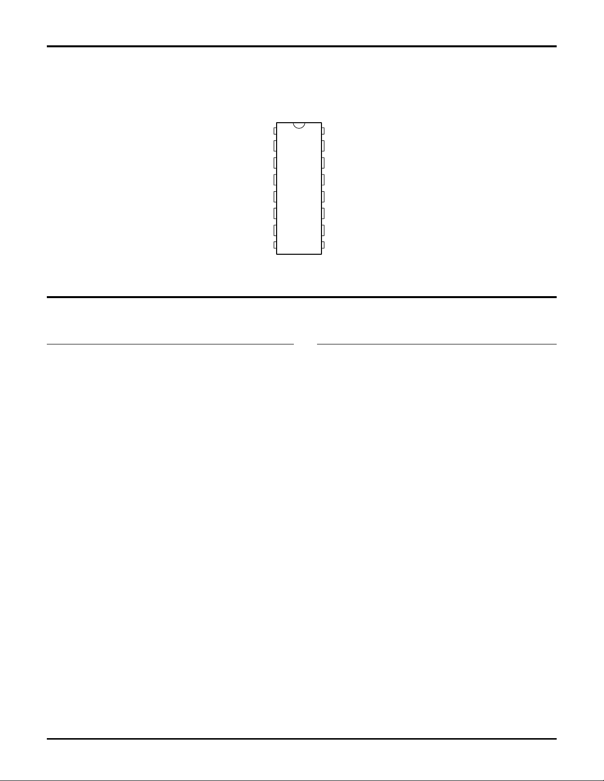
PIN CONFIGURATION
ML4800
16-Pin PDIP (P16)
16-Pin Narrow SOIC (S16N)
PIN DESCRIPTION
PIN NAME FUNCTION
1 IEAO Slew rate enhanced PFC
transconductance error amplifier output
2I
AC
3I
SENSE
PFC AC line reference input to Gain
Modulator
Current sense input to the PFC Gain
Modulator
IEAO
I
AC
I
SENSE
V
RMS
V
DC
RAMP 1
RAMP 2
SS
1
2
3
4
5
6
7
8
TOP VIEW
16
VEAO
15
V
FB
14
V
REF
13
V
CC
12
PFC OUT
11
PWM OUT
10
GND
9
DC I
LIMIT
PIN NAME FUNCTION
9 DC I
LIMIT
PWM cycle-by-cycle current limit
comparator input
10 GND Ground
11 PWM OUT PWM driver output
12 PFC OUT PFC driver output
4V
RMS
PFC Gain Modulator RMS line voltage
compensation input
5 SS Connection point for the PWM soft start
capacitor
6V
DC
PWM voltage feedback input
7 RAMP 1 Oscillator timing node; timing set
by R
TCT
8 RAMP 2 When in current mode, this pin
functions as the current sense input;
when in voltage mode, it is the PWM
modulation ramp input.
13 V
14 V
CC
REF
Positive supply
Buffered output for the internal
7.5V reference
15 V
FB
PFC transconductance voltage
error amplifier input
16 VEAO PFC transconductance voltage
error amplifier output
2 REV. 1.0.2 3/7/2001
ABSOLUTE MAXIMUM RATINGS
ML4800
Absolute maximum ratings are those values beyond which
the device could be permanently damaged. Absolute
maximum ratings are stress ratings only and functional
device operation is not implied.
Junction Temperature.............................................. 150°C
Storage Temperature Range ...................... -65°C to 150°C
Lead Temperature (Soldering, 10 sec) ..................... 260°C
Thermal Resistance (θ
)
JA
Plastic DIP .......................................................... 80°C/W
V
..............................................................................................
CC
Voltage ................................................. -5V to 0.7V
I
SENSE
Voltage on Any Other Pin ...... GND - 0.3V to V
I
...........................................................................................
REF
I
Input Current .................................................... 10mA
AC
CCZ
18V
+ 0.3V
10mA
Peak PFC OUT Current, Source or Sink ....................... 1A
Peak PWM OUT Current, Source or Sink .................... 1A
Plastic SOIC ...................................................... 105°C/W
OPERATING CONDITIONS
Temperature Range
ML4800CX.................................................... 0°C to 70°C
ML4800IX .................................................. -40°C to 85°C
PFC OUT, PWM OUT Energy Per Cycle ................... 1.5µJ
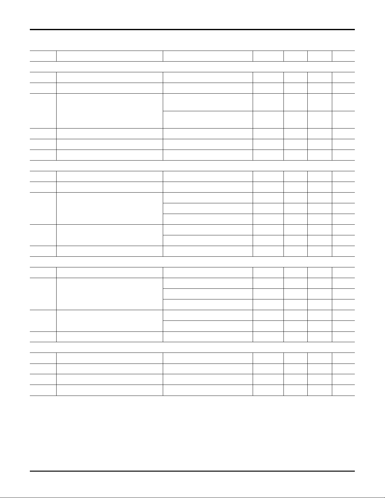
ELECTRICAL CHARACTERISTICS
Unless otherwise specified, VCC = 15V, RT = 52.3kΩ, CT = 470pF, TA = Operating Temperature Range (Note 1)
SYMBOL PARAMETER CONDITIONS MIN TYP MAX UNITS
VOLTAGE ERROR AMPLIFIER
Input Voltage Range 0 5 V
Transconductance V
Feedback Reference Voltage 2.43 2.5 2.57 V
NON INV
= V
, VEAO = 3.75V 30 65 90 µ
INV
Ω
Input Bias Current Note 2 -0.5 -1.0 µA
Output High Voltage 6.0 6.7 V
Output Low Voltage 0.1 0.4 V
Source Current VIN = ±0.5V, V
Sink Current VIN = ±0.5V, V
Open Loop Gain 50 60 dB
Power Supply Rejection Ratio 11V < VCC < 16.5V 50 60 dB
CURRENT ERROR AMPLIFIER
Input Voltage Range -1.5 2 V
Transconductance V
Input Offset Voltage 0 4 15 mV
Input Bias Current -0.5 -1.0 µA
Output High Voltage 6.0 6.7 V
Output Low Voltage 0.65 1.0 V
Source Current VIN = ±0.5V, V
Sink Current VIN = ±0.5V, V
Open Loop Gain 60 70 dB
Power Supply Rejection Ratio 11V < VCC < 16.5V 60 75 dB
OVP COMPARATOR
NON INV
= 6V -40 -140 µA
OUT
= 1.5V 40 140 µA
OUT
= V
, VEAO = 3.75V 50 100 150 µ
INV
= 6V -40 -104 µA
OUT
= 1.5V 40 160 µA
OUT
Ω
Threshold Voltage 2.65 2.75 2.85 V
Hysteresis 175 250 325 mV
REV. 1.0.2 3/7/2001 3
ML4800
ELECTRICAL CHARACTERISTICS
SYMBOL PARAMETER CONDITIONS MIN TYP MAX UNITS
TRI-FAULT DETECT
Fault Detect HIGH 2.65 2.75 2.85 V
Time to Fault Detect HIGH V
= V
FB
FAULT DETECT LOW
OPEN. 470pF from VFB to GND
Fault Detect LOW 0.4 0.5 0.6 V
to VFB =24ms
PFC I
COMPARATOR
LIMIT
Threshold Voltage -0.9 -1.0 -1.1 V
(PFC I
LIMIT VTH
Delay to Output 150 300 ns
DC I
COMPARATOR
LIMIT
Threshold Voltage 0.95 1.0 1.05 V
Input Bias Current ±0.3 ±1 µA
Delay to Output 150 300 ns
VIN OK COMPARATOR
Threshold Voltage 2.35 2.45 2.55 V
Hysteresis 0.8 1.0 1.2 V
GAIN MODULATOR
Gain (Note 3) IAC = 100µA, V
Bandwidth IAC = 100µA 10 MHz
Output Voltage I
- Gain Modulator Output) 120 220 mV
= VFB = 0V 0.60 0.80 1.05
RMS
IAC = 50µA, V
IAC = 50µA, V
IAC = 100µA, V
= 350µA, V
AC
= 1.2V, VFB = 0V 1.8 2.0 2.40
RMS
= 1.8V, VFB = 0V 0.85 1.0 1.25
RMS
= 3.3V, VFB = 0V 0.20 0.30 0.40
RMS
= 1V, 0.60 0.75 0.9 V
RMS
VFB = 0V
OSCILLATOR
Initial Accuracy TA = 25°C 717681kHz
Voltage Stability 11V < VCC < 16.5V 1 %
Temperature Stability 2%
Total Variation Line, Temp 68 84 kHz
Ramp Valley to Peak Voltage 2.5 V
PFC Dead Time 250 330 ns
CT Discharge Current V
RAMP 2
= 0V, V
= 2.5V 3.5 5.5 7.5 mA
RAMP 1
4 REV. 1.0.2 3/7/2001
ML4800
ELECTRICAL CHARACTERISTICS
SYMBOL PARAMETER CONDITIONS MIN TYP MAX UNITS
REFERENCE
PFC
PWM
Output Voltage TA = 25°C, I(V
) = 1mA 7.4 7.5 7.6 V
REF
Line Regulation 11V <VCC <16.5V 10 25 mV
Load Regulation 0mA <I(V
) <10mA;
REF
TA = 0ºC to 70ºC 10 20 mV
0mA < I(V
) < 5mA;
REF
TA = –40ºC to 85ºC 10 20 mV
Temperature Stability 0.4 %
Total Variation Line, Load, Temp 7.35 7.65 V
Long Term Stability TJ = 125°C, 1000 Hours 5 25 mV
Minimum Duty Cycle V
Maximum Duty Cycle V
Output Low Voltage I
Output High Voltage I
> 4.0V 0 %
IEAO
< 1.2V 90 95 %
IEAO
= -20mA 0.4 0.8 V
OUT
I
= -100mA 0.7 2.0 V
OUT
I
= 10mA, VCC = 9V 0.4 0.8 V
OUT
= 20mA V
OUT
I
= 100mA V
OUT
– 0.8V V
CC
- 2V V
CC
Rise/Fall Time CL = 1000pF 50 ns
Duty Cycle Range 0-44 0-47 0-49 %
Output Low Voltage I
Output High Voltage I
= -20mA 0.4 0.8 V
OUT
I
= -100mA 0.7 2.0 V
OUT
I
= 10mA, VCC = 9V 0.4 0.8 V
OUT
= 20mA V
OUT
I
= 100mA V
OUT
Rise/Fall Time CL = 1000pF 50 ns
SUPPLY
Start-up Current VCC = 12V, CL = 0 200 350 µA
Operating Current 14V, CL = 0 5.5 7 mA
Undervoltage Lockout Threshold 12.4 13 13.6 V
Undervoltage Lockout Hysteresis 2.5 2.8 3.1 V
Note 1: Limits are guaranteed by 100% testing, sampling, or correlation with worst-case test conditions.
Note 2: Includes all bias currents to other circuits connected to the V
Note 3: Gain = K x 5.3V; K = (I
GAINMOD
- I
) x [IAC (VEAO - 0.625)]-1; VEAO
OFFSET
pin.
FB
MAX
=5V.
– 0.8V V
CC
- 2V V
CC
REV. 1.0.2 3/7/2001 5
 Loading...