

Fairchild Semiconductor ML2035C Datasheet
February 1997
ML2035
Serial Input Programmable Sine Wave Generator
GENERAL DESCRIPTION
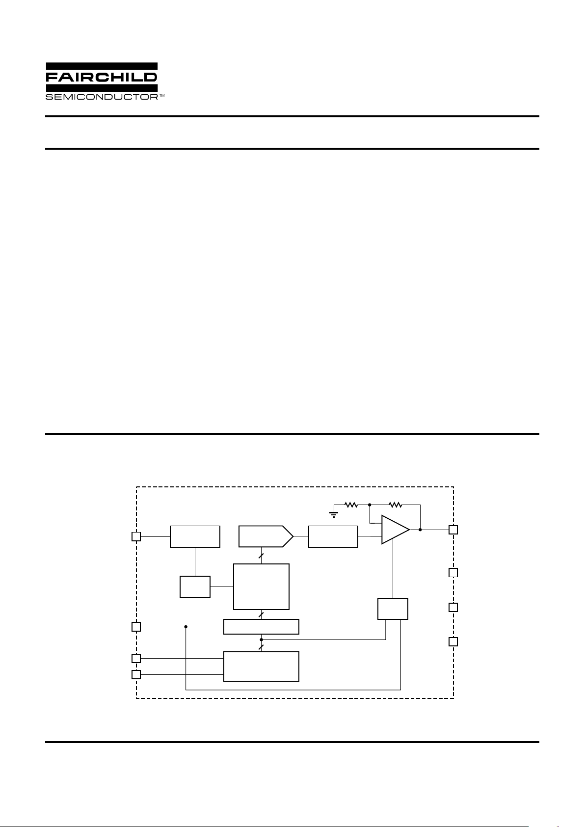
The ML2035 is a monolithic sinewave generator whose
output is programmable from DC to 25kHz. No external
components are required. The frequency of the sinewave
output is derived from either an external crystal or clock
input, providing a stable and accurate frequency
reference. The frequency is programmed by a 16-bit serial
data word. The ML2035 has a V
OUT
amplitude of ±VCC/2.
The ML2035 is intended for telecommunications and
modem applications that need low cost and accurate
generation of precise test tones, call progress tones, and
signaling tones.
BLOCK DIAGRAM
FEATURES
■ Programmable output frequency - DC to 25kHz
■ Low gain error and total harmonic distortion
■ 3-wire SPI compatible serial microprocessor interface
with double buffered data latch
■ Fully integrated solution - no external components
required
■ Frequency resolution of 1.5Hz (±0.75Hz) with a
12MHz clock input
■ Onboard 3 to 12MHz crystal oscillator
■ Synchronous or asynchronous data loading capability
■ Compatible with ML2031 and ML2032 tone detectors
and ML2004 logarithmic gain/attenuator
V
OUT
LATI
SCK
SID
4
2
3
6
8-BIT
DAC
PHASE
ACCUMULATOR
& 512 POINT
SINE LOOK-UP
TABLE
8
16
16
16-BIT DATA LATCH
16-BIT SHIFT REGISTER
CRYSTAL
OSCILLATOR
÷4
CLK IN
8
GND
7
V
CC
5
V
SS
1
-
+
5kΩ 5kΩ
ZERO
DETECT
SMOOTHING
FILTER
REV. 1.0 10/10/2000

ML2035
2 REV. 1.0 10/10/2000
PIN CONFIGURATION
PIN DESCRIPTION
PIN NAME FUNCTION
1V
SS
Negative supply (-5V).
2 SCK Serial clock. Digital input which
clocks in serial data on its rising
edges.
3 SID Serial input data which programs the
frequency of V
OUT
.
4 LATI Digital input which latches serial data
into the internal data latch on falling
edges.
PIN NAME FUNCTION
5V
CC
Positive supply (5V).
6V
OUT
Analog output. V
OUT
swing is ±VCC/2.
7 GND Ground. All inputs and outputs are
referenced to this point.
8 CLK IN Clock input. The internal clock can be
generated by tying a 3 to 12MHz
crystal from this pin to GND, or
applying a digital clock signal directly
to the pin.
1
2
3
4
8
7
6
5
V
SS
SCK
SID
LATI
CLK IN
GND
V
OUT
V
CC
TOP VIEW
ML2035
8-Pin PDIP (P08)
ML2035
REV. 1.0 10/10/2000 3
ELECTRICAL CHARACTERISTICS
Unless otherwise specified, VCC = 4.5V to 5.5V, VSS = -4.5V to -5.5V, CLK IN = 12.352MHz, CL = 100pF, RL = 1kΩ,
T
A
= Operating Temperature Range (Note 1)
SYMBOL PARAMETER CONDITIONS MIN TYP MAX UNITS
OUTPUT
HD Harmonic Distortion 20Hz to 5kHz -45 dB
(2nd and 3rd Harmonic) 5kHz to 25kHz -40 dB
SND Signal to Noise + Distortion 200Hz to 3.4kHz, -45 dB
f
OUT
BW = 20Hz to 4kHz
20Hz to 25kHz, -40 dB
f
OUT
BW = 20 Hz to 75kHz
V
GN
Gain Error 20Hz < f
OUT
< 5kHz ±0.15 dB
5kHz < f
OUT
< 25kHz ±0.3 dB
ICN Idle Channel Noise Power Down Mode, Cmsg Weighted -20 0 dBrnc
Power Down Mode, 1kHz 50 nV/ Hz
PSRR Power Supply Rejection Ratio 200mV
P-P
, 0 - 10kHz V
CC
-40 dB
Sine, Measured on V
OUT
V
SS
-40 dB
V
OS
V
OUT
Offset Voltage ±75 mV
V
P-P
Peak-to-Peak Output Voltage ±VCC/2 V
OSCILLATOR
VIL CLK CLK IN Input Low Voltage 1.5 V
VIH CLK CLK IN Input High Voltage 3.5 V
IIL CLK CLK IN Input Low Current -250 µA
IIH CLK CLK IN Input High Current 250 µA
CIN CLK CLK IN Input Capacitance 12 pF
t
CKI
CLK IN On/Off Period tR = tF = 10ns, 2.5V Midpoint 30 ns
LOGIC (LATI, SID, SCK)
V
IL
Input Low Voltage 0.8 V
V
IH
Input High Voltage 2.0 V
I
IL
Input Low Current VIN = 0V -1 µA
I
IH
Input High Current VIN = V
CC
1 µA
ABSOLUTE MAXIMUM RATINGS
Absolute maximum ratings are those values beyond which
the device could be permanently damaged. Absolute
maximum ratings are stress ratings only and functional
device operation is not implied.
V
CC
.............................................................................................
6.5V
V
SS
............................................................................................
-6.5V
V
OUT
...................................................
VSS - 0.3V to VCC + 0.3V
Voltage on any other pin ........ GND - 0.3V to V
CC
+ 0.3V
Input Current........................................................ ±25mA
Junction Temperature ............................................. 150ºC
Storage Temperature Range ......................–65ºC to 150ºC
Lead Temperature (Soldering, 10 sec) ..................... 260ºC
Thermal Resistance (θ
JA
).....................................110ºC/W
OPERATING CONDITIONS
Temperature Range
ML2035CP .................................................0ºC to 70ºC
ML2035IP ............................................... -40ºC to 85ºC
V
CC
Range ................................................... 4.5V to 5.5V
V
SS
Range ..................................................-4.5V to -5.5V
 Loading...