

Fairchild Semiconductor LM431B, LM431A, LM431C Datasheet
LM431A/LM431B/LM431C
Programmable Shunt Regulator
www.fairchildsemi.com
Features
• Programmable Output Voltage to 36 Volts
• Low Dynamic Output Impedance 0.20 Typical
• Sink Curren t Capability of 1.0 to 100mA
• Equivalent Full-Range Temperature Coefficient of
50ppm/°C Typical
• Temperature Compensated for Operation Over Full Rated
Operating Temperature Range
• Low Output Noise Voltage
• Fast Turn-on Response
Description
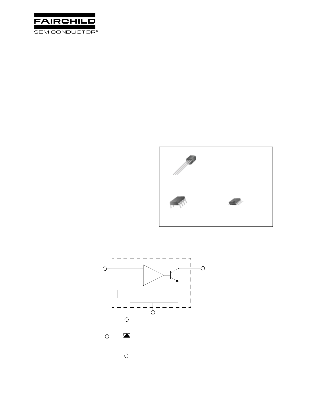
The LM431A/LM431B/LM431C are three terminal output
adjustable regulators with thermal stability over operating
temperature range. The output voltage can be set any value
between V
two external resistors. These devices have a typical dynamic
output imped ance of 0.2Ω Act ive output circ uit provides a
sharp turn-on characteristic, making these devices excellent
replacement for Zener Diodes in many applications.
TO-92
1
1. Ref 2. Anode 3. Cathode
8-DIP 8-SOP
1.Cathode 2.3 .4.5.7.NC
6.Anode 8.Ref
(approximately 2.5 volts) and 36 volts with
REF
1
1.Cathode 2.3.6.7.A no de
4.5.NC 8.Ref
1
Internal Block Diagram
REFERENCE
REFERENCE (R)
©2002 Fairchild Semiconductor Corporation
CATHODE
2.5 Vref
ANODE
CA THODE (K)
ANODE (A)
Rev. 1.0.6
LM431A/LM431B/LM431C
Absolute Maximum Ratings
(Operating temperature range applies unless otherwise specified.)
Parameter Symbol Value Unit
Cathode Voltage V
Cathode Current Range (Continuous) I
Reference Input Current Range I
KA
KA
REF
37 V
-100 ~ +150 mA
0.05 ~ +10 mA
Power Dissipation
M, Z Suffix Package
N Suffix Package
P
D
770
mW
1000
Operating Temperature Range
LM431xC
LM431xI -40 ~ +85 °C
Junction Temperature T
Storage Temperature Range T
T
OPR
J
STG
-25 ~ +85 °C
150 °C
-65 ~ +150 °C
Recommended Operating Conditions
Parameter Symbol Min Typ Max Unit
Cathode Voltage V
Cathode Current I
KA
KA
V
REF
1.0 - 100 mA
-36V
2

Electrical Characteristics
(TA = +25°C, unless otherwise specified)
LM431A/LM431B/LM431C
Parameter Symbol Conditions
Reference
Input Voltage
Deviation of
Reference
Input Voltage
OverTemperature
Ratio of
Change in
Reference
Input Voltage
to the Change
in Cathode
Voltage
Reference
Input Current
Deviation of
Reference
Input Current
Over Full
Temperature
Range
Minimum
Cathode Current for
Regulation
Off - Stage
Cathode
Current
Dynamic
Impedance Z
V
REF
V
∆
∆
V
∆
V
∆
I
REF
I
∆
REF
I
KA(MIN)VKA=VREF
I
KA(OFF)
REF
T
REF
KA
/
/
/∆T
V
= V
KA
V
KA=VREF
T
MIN≤TA≤TMAX
IKA
=10mA
IKA=10mA,
=10kΩ,R2=∞
R
1
I
=10mA,
KA
=10kΩ,R2=∞
R
1
T
=Full Range
A
VKA=36V,
V
=0
REF
VKA=V
KA
KA
=1 to 100mA
I
f ≥1.0kHz
, I
REF
, IKA=10mA
∆
V
∆
10V
,
REF
KA
VKA=10V-
REF
VKA=36V-
LM431A LM431B LM431C
Min. Typ. Max. Min. Typ. Max. Min. Typ. Max.
Unit
=10mA 2.450 2.500 2.550 2.470 2.495 2.520 2.482 2.495 2.508 V
-
4.5 17
-
4.5 17
-
4.5 17 mV
- -1.0 -2.7 - -1.0 -2.7 - -1.0 -2.7
mV/V
- -0.5 -2.0 - -0.5 -2.0 - -0.5 -2.0
-1.54 -1.54 -1.54
-
0.4 1.2
-
0.4 1.2
-
0.4 1.2
µ
µ
- 0.45 1.0 - 0.45 1.0 - 0.45 1.0 mA
- 0.05 1.0 - 0.05 1.0 - 0.05 1.0
µ
- 0.15 0.5 - 0.15 0.5 - 0.15 0.5 Ω
A
A
A
Note1
•LM431
•LM431
C : T
X
I : T
X
MIN
MIN
= -25 °C, T
= -40°C, T
MAX
MAX
= +85°C
= +85°C
3
LM431A/LM431B/LM431C
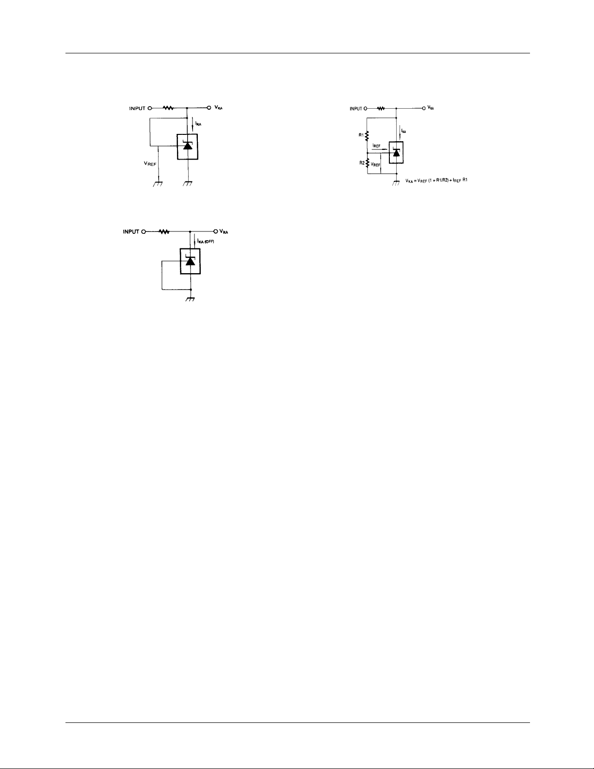
Test Circuits
LM431A/B/C
LM431A/B/C
Figure 1. Test Circuit for VKA=V
LM431A/B/C
Figure 3. Test Circuit for l
KA(OFF)
REF
Figure 2. Test Circuit for V
KA
≥≥≥≥V
REF
4
 Loading...