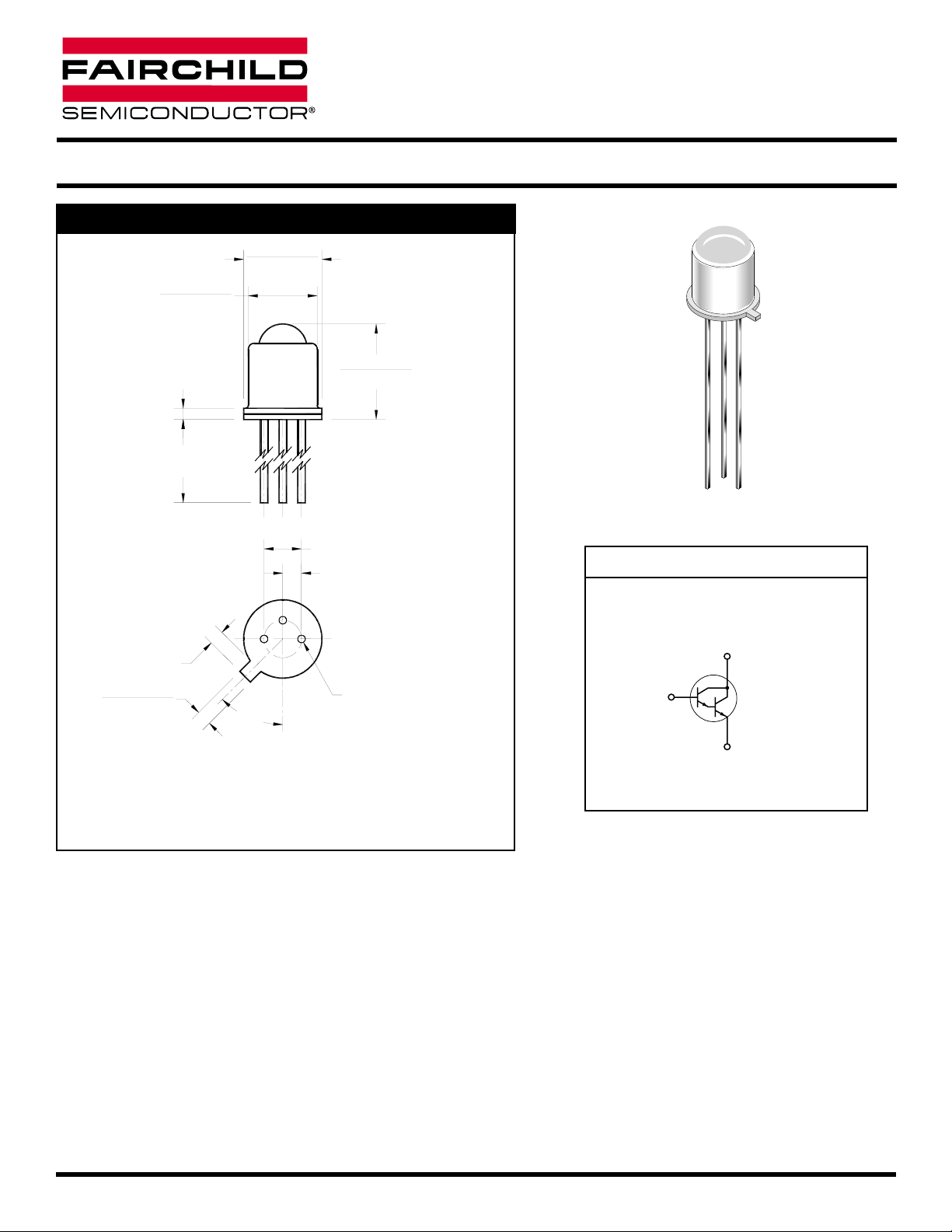
0.038 (0.97)
0.100 (2.54)
0.050 (1.27)
45°
0.046 (1.16)
0.036 (0.92)
13
0.030 (0.76)
NOM
0.195 (4.95)
0.178 (4.52)
0.230 (5.84)
0.209 (5.31)
0.500 (12.7)
MIN
0.255 (6.47)
0.225 (5.71)
Ø0.020 (0.51) 3X
2
PACKAGE DIMENSIONS
FEATURES
• Hermetically sealed package
• Narrow reception angle
NOTES:
1. Dimensions for all drawings are in inches (mm).
2. Tolerance of ± .010 (.25) on all non-nominal dimensions
unless otherwise specified.
DESCRIPTION
The L14F1/L14F2 are silicon photodarlingtons mounted in a narrow angle, TO-18 package.
2001 Fairchild Semiconductor Corporation
DS300306 6/01/01 1 OF 4 www.fairchildsemi.com
SCHEMATIC
HERMETIC SILICON
PHOTODARLINGTON
L14F1 L14F2
BASE 2
(CONNECTED TO CASE)
COLLECTOR
3
1
EMITTER

www.fairchildsemi.com 2 OF 4 6/01/01 DS300306
PARAMETER TEST CONDITIONS SYMBOL MIN TYP MAX UNITS
Collector-Emitter Breakdown IC= 10 mA, Ee = 0 BV
CEO
25 — V
Emitter-Base Breakdown IE= 100 µA, Ee = 0 BV
EBO
12 — V
Collector-Base Breakdown IC= 100 µA, Ee = 0 BV
CBO
25 — V
Collector-Emitter Leakage VCE= 12 V, Ee = 0 I
CEO
— 100 nA
Reception Angle at 1/2 Sensitivity θ ±8 Degrees
On-State Collector Current L14F1 Ee = .125 mW/cm2, VCE= 5 V
(7)
I
C(ON)
7.5 — mA
On-State Collector Current L14F2 Ee = .125 mW/cm2, VCE= 5 V
(7)
I
C(ON)
2.5 mA
Rise Time IC= 10 mA, VCC= 5 V, RL=100 Ω t
r
300 µs
Fall Time IC= 10 mA, VCC= 5 V, RL=100 Ω t
f
250 µs
ELECTRICAL / OPTICAL CHARACTERISTICS
(TA =25°C) (All measurements made under pulse conditions)
Parameter Symbol Rating Unit
Operating Temperature T
OPR
-65 to +125 °C
Storage Temperature T
STG
-65 to +150 °C
Soldering Temperature (Iron)
(3,4,5 and 6)
T
SOL-I
240 for 5 sec °C
Soldering Temperature (Flow)
(3,4 and 6)
T
SOL-F
260 for 10 sec °C
Collector to Emitter Breakdown Voltage
V
CEO
25 V
Collector to Base Breakdown Voltage V
CBO
25 V
Emitter to Base Breakdwon Voltage V
EBO
12 V
Power Dissipation(TA= 25°C)
(1)
P
D
300 mW
Power Dissipation(TC= 25°C)
(2)
P
D
600 mW
ABSOLUTE MAXIMUM RATINGS
(TA= 25°C unless otherwise specified)
NOTE:
1. Derate power dissipation linearly 3.00 mW/°C above 25°C ambient.
2. Derate power dissipation linearly 6.00 mW/°C above 25°C case.
3. RMA flux is recommended.
4. Methanol or isopropyl alcohols are recommended as cleaning agents.
5. Soldering iron tip
1/16” (1.6mm) minimum from housing.
6. As long as leads are not under any stress or spring tension.
7. Light source is a GaAs LED emitting light at a peak wavelength of 940 nm.
8. Figure 1 and figure 2 use light source of tungsten lamp at 2870°K color temperature. A GaAs source of 0.05 mW/cm
2
is approximately
equivalent to a tungsten source, at 2870°K, of 0.2 mW/cm
2
.
L14F1 L14F2
HERMETIC SILICON
PHOTODARLINGTON
 Loading...