

Fairchild Semiconductor KST5551 Datasheet
©2003 Fairchild Semiconductor Corporation Rev. B2, February 2003
KST5551
NPN Epitaxial Silicon Transistor
Absolute Maximum Ratings
Ta=25°C unless otherwise noted
• Refer to 2N5551 for graphs
Electrical Characteristics
Ta=25°C unless otherwise noted
* Pulse Test: Pulse Width=300µs, Duty Cycle=2%
Symbol Parameter Value Units
V
CBO
Collector-Base Voltage 180 V
V
CEO
Collector-Emitter Voltage 160 V
V
EBO
Emitter-Base Voltage 6 V
I
C
Collector Current 600 mA
P
C
Collector Power Dissipation 350 mW
T
J
Junction Temperature 150 °C
T
STG
Storage Temperature -55 ~ 150 °C
Symbol Parameter Test Condition Min. Max. Units
BV
CBO
Collector-Base Breakdown Voltage IC=100µA, IE=0 180 V
BV
CEO
Collector-Emitter Breakdown Voltage IC=1mA, IB=0 160 V
BV
EBO
Emitter-Base Breakdown Voltage IE=10µA, IC=0 6 V
I
CBO
Collector Cut-off Current VCB=120V, IE=0 50 nA
I
EBO
Emitter Cut-off Current VEB=4V, IC=0 50 nA
h
FE
DC Current Gain VCE=5V, IC=1mA
V
CE
=5V, IC=10mA
V
CE
=5V, IC=50mA
80
80
30
250
V
CE
(sat) Collector-Emitter Saturation Voltage IC=10mA, IB=1mA
I
C
=50mA, IB=5mA
0.15
0.2
V
V
V
BE
(sat) Base-Emitter Saturation Voltage IC=10mA, IB=1mA
I
C
=50mA, IB=5mA
1
1
V
V
f
T
Current Gain Bandwidth Product VCE=10V, IC=10mA,
f=100MHz
100 300 MHz
C
ob
Output Capacitance VCB=10V, IE=0, f=1MHz 6 pF
NF Noise Figure V
CE
=5V, IC=250µA, RS=1KΩ,
f=10Hz to 15.7KMz
8dB
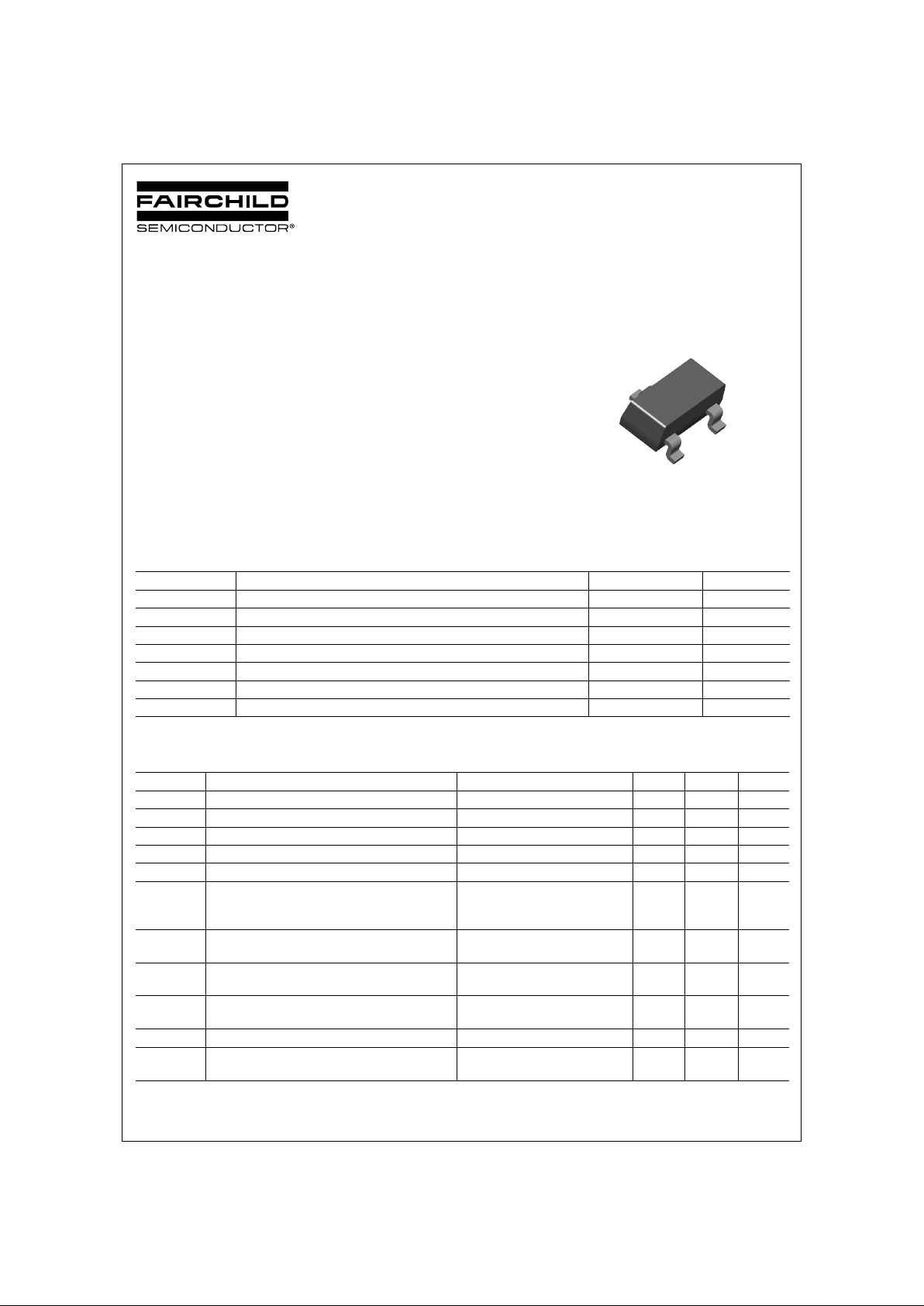
KST5551
Amplifier Transistor
• Collector-Emitter Voltage: V
CEO
=160V
• Collector Power Dissipation: P
C
(max)=350mW
1. Base 2. Emitter 3. Collector
SOT-23
1
2
3
Mark: G1
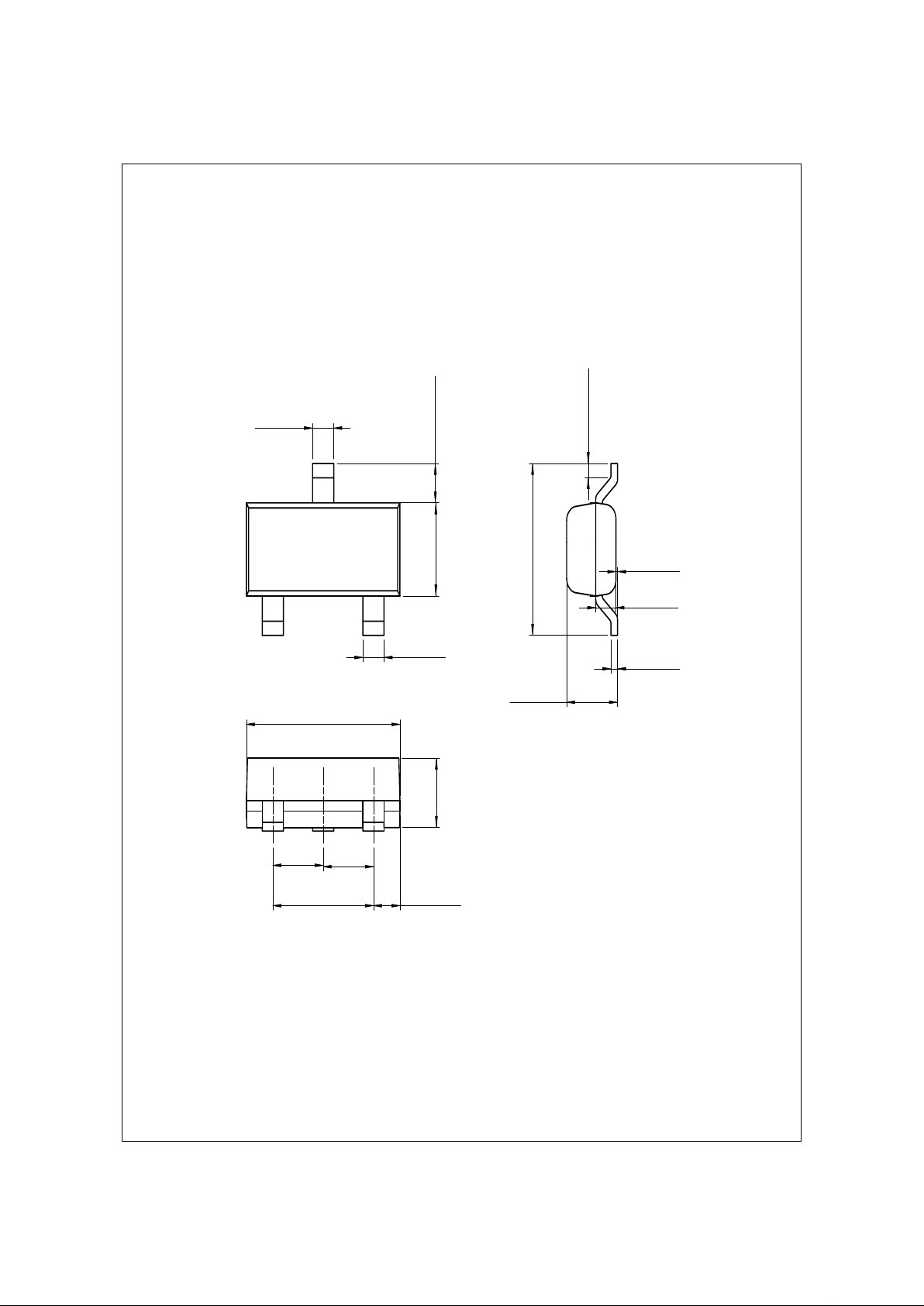
0.96~1.14
0.12
0.03~0.10
0.38 REF
0.40
±0.03
2.90
±0.10
0.95
±0.03
0.95
±0.03
1.90
±0.03
0.508REF
0.97REF 1.30
±0.10
0.45~0.60
2.40
±0.10
+0.05
–0.023
0.20 MIN
0.40
±0.03
SOT-23
Package Dimensions
KST5551
Rev. B2, February 2003
Dimensions in Millimeters
©2003 Fairchild Semiconductor Corporation
 Loading...