

KSC2751
High Speed
High Current Switching Industrial Use
KSC2751
TO-3P
NPN Epitaxial Silicon Transistor
Absolute Maximum Ratings
TC=25°C unless otherwise noted
1
1.Base 2.Collector 3.Emitter
Symbol Parameter Value Units
V
CBO
V
CEO
VEBO
IC
ICP
IB
PC
T
J
T
STG
* PW≤300µs, Duty Cycle≤10%
Electrical Characteristics
Collector-Base Voltage 500 V
Collector-Emitter Voltage 400 V
Emitter-Base Voltage 7 V
Collector Current (DC) 15 A
*Collector Current (Pulse) 30 A
Base Current (DC) 7.5 A
Collector Dissipation (TC=25°C) 120 W
Junction Temperature 150 °C
Storage T emperature - 55 ~ 150 °C
TC=25°C unless otherwise noted
Symbol Parameter Test Condition Min Typ Max Units
(sus) Collector-Emitter Sustaining V olt age IC = 10A, IB1= 2A, L = 50µH 400 V
V
CEO
V
(sus)1 Collector-Emitter Sustaining Voltage IC = 10A, IB1= -IB2 = 2A
CEX
V
(sus)2 Collector-Emitter Sustaining Voltage IC = 20A, IB1 = 4A, -IB2 = 2A
CEX
I
CBO
I
CER
I
CEX1
ICEX2
I
EBO
h
FE1
h
FE2
h
FE3
(sat) * Collector-Emitter Saturation Voltage IC = 10A, IB = 2A 0.3 1 V
V
CE
(sat) * Base Emitter ON Voltage IC = 10A, IB = 2A 1 1.5 V
V
BE
tON
tSTG
tF
* Pulse Test: PW≤350µs, Duty Cycle≤2% Pulsed
Collector Cut-off Current V
Collector Cut-off Current V
Collector Cut-off Curren V
Collector Cut-off Current V
Emitter Cut-off Current V
* DC Current Gain V
Turn ON Time V
Storage Time 2.5 µs
Fall Time 0.7 µs
=125°C, l = 180µH, Clamped
T
C
= 125°C, L = 180µH,Clamped
T
C
= 400V, IE = 0 100 µA
CB
= 400V, R
CE
T
= 125°C
C
= 400V, VBE(off) = -1.5 V 100 µA
CE
= 400V, VBE(off) = -1.5 V @
CE
= 125Ω
T
C
= 5V, IC = 0 10 µA
EB
= 5V, IC = 2A
CE
= 5V, IC = 5A
V
CE
V
= 5V, IC = 10A
CE
= 150V, IC = 10A
CC
= -IB2 = 2A
I
B1
= 15Ω
R
L
= 50Ω @
BE
450 V
400 V
2 mA
1mA
15
35 80
10
7
1 µs
hFE Classificntion
Classification N R O Y
h
FE1
©2000 Fairchild Semiconductor International Rev. A, February 2000
15 ~ 30 20 ~ 40 30 ~ 60 40 ~ 80
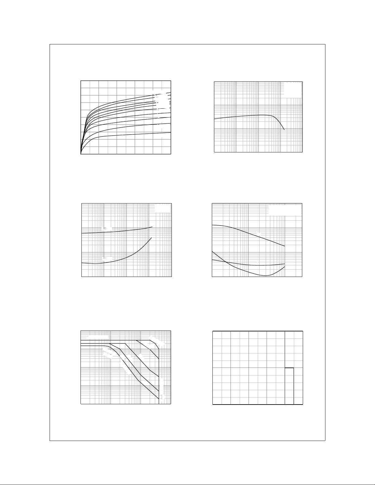
Typical Characteristics
KSC2751
20
18
16
14
12
10
8
6
[A], COLLECTOR CURRENT
4
C
I
2
0
012345
IB = 2.0A
IB = 1.8A
IB = 1.6A
IB = 1.4A
IB = 1.2A
IB = 1.0A
IB = 0.8A
IB = 0.6A
IB = 0.4A
IB = 0.2A
VCE[V], CO LLEC T OR-EM ITTER VOLTAGE
Figure 1. Static Characteristic Figure 2. DC current Gain
10
1
0.1
(sat)[V], SATURATION VOLTAGE
CE
(sat), V
BE
V
0.01
0.01 0.1 1 10 100
VBE(sat)
VCE(sat)
IC[A], COLLECTOR CURRENT
IC = 5 I
1000
100
10
, DC CURRENT GAIN
FE
h
1
0.01 0.1 1 10 100
VCE = 5V
Pulsed
IC[A], COLLECTOR CURRENT
100
B
10
s], TIME
µ
[
F
, t
STG
, t
1
ON
t
0.1
0.1 1 10
t
STG
t
F
t
ON
IC = 5 IB1 = -5 I
Pulsed, VCC = 150V
B2
IC[A], COLLECTOR CURRENT
Figure 3. Base-Emitter Saturation Voltage
Collector-Emitter Saturation Voltage
100
IC(Pulse) MAX.
10
1
0.1
[A], COLLECTOR CURRENT
C
I
0.01
1 10 100 1000
Dissipation
Limited
VCE[V], COLLECTOR-EMITTER VOLTAGE
Figure 5. Safe Operating Area Figure 6. Reverse Bias Safe Operating Area
©2000 Fairchild Semiconductor International
DC
S/b Limited
Figure 4. Switching Time
20
PW = 10us
100us
1ms
10ms
(sus) MAX.
CEO
V
10
[A], COLLECTOR CURRENT
C
I
0
0 100 200 300 400 500
VCE[V], COLLECTOR-EMITTER VOLTAGE
(sus)
(sus)
CEX
CEO
V
V
Rev. A, February 2000
 Loading...