Fairchild Semiconductor KA78T15TU, KA78T12TU, KA78T12, KA78T05TU, KA78T05 Datasheet

©2001 Fairchild Semiconductor Corporation
www.fairchildsemi.com
Rev. 1.0.0
Features
• Output current in excess of 3.0A
• Output transistor safe operating area compensation
• Power dissipation :25W
• Internal short circuit current limiting
• Internal thermal overload protection
• Output voltage offered in 4% tolerance
• No external components required
• Output voltage of 5, 12 and 15V
Description
This family of fixed voltage regulators are monolithic
integrated circuit capable of driving loads in excess of 3.0 A.
TO-220
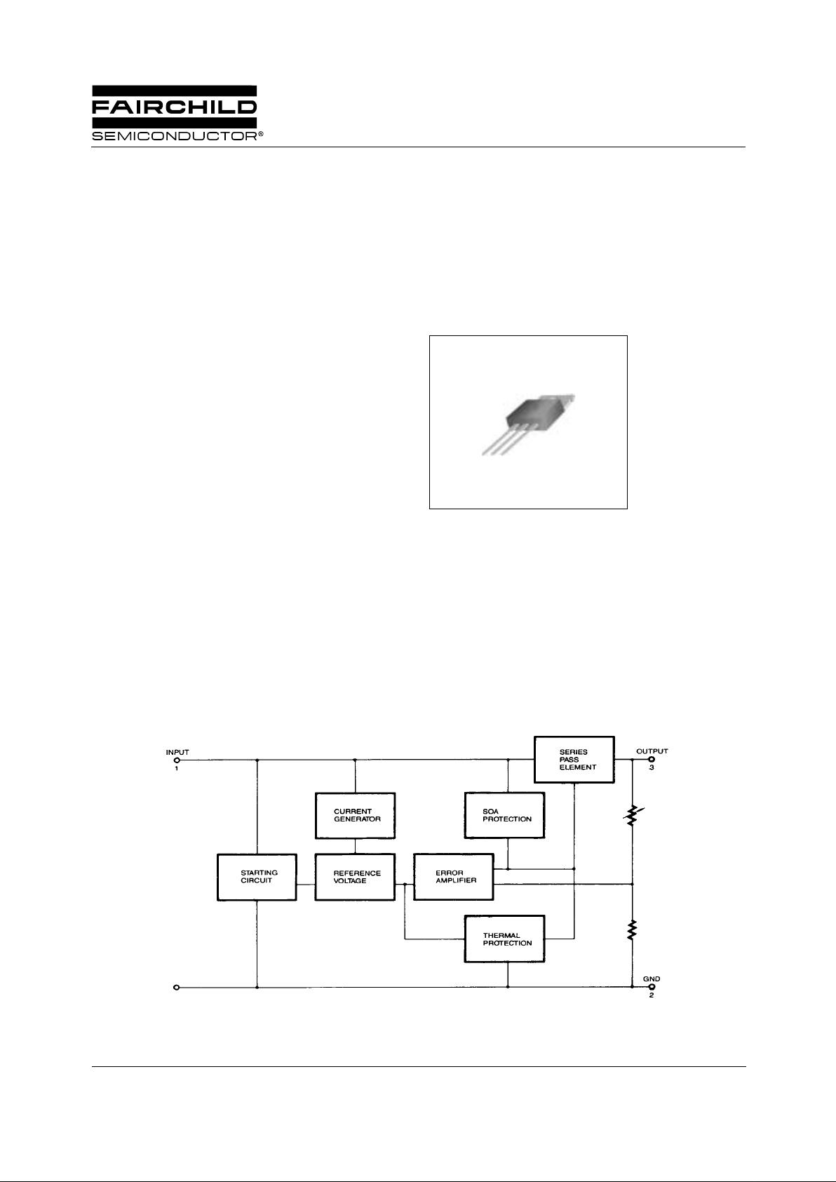
1.Input 2. GND 3. Output
1
Internal Block Diagram
KA78TXX
3-Terminal 3A Positive Voltage Regulator

KA78TXX
2
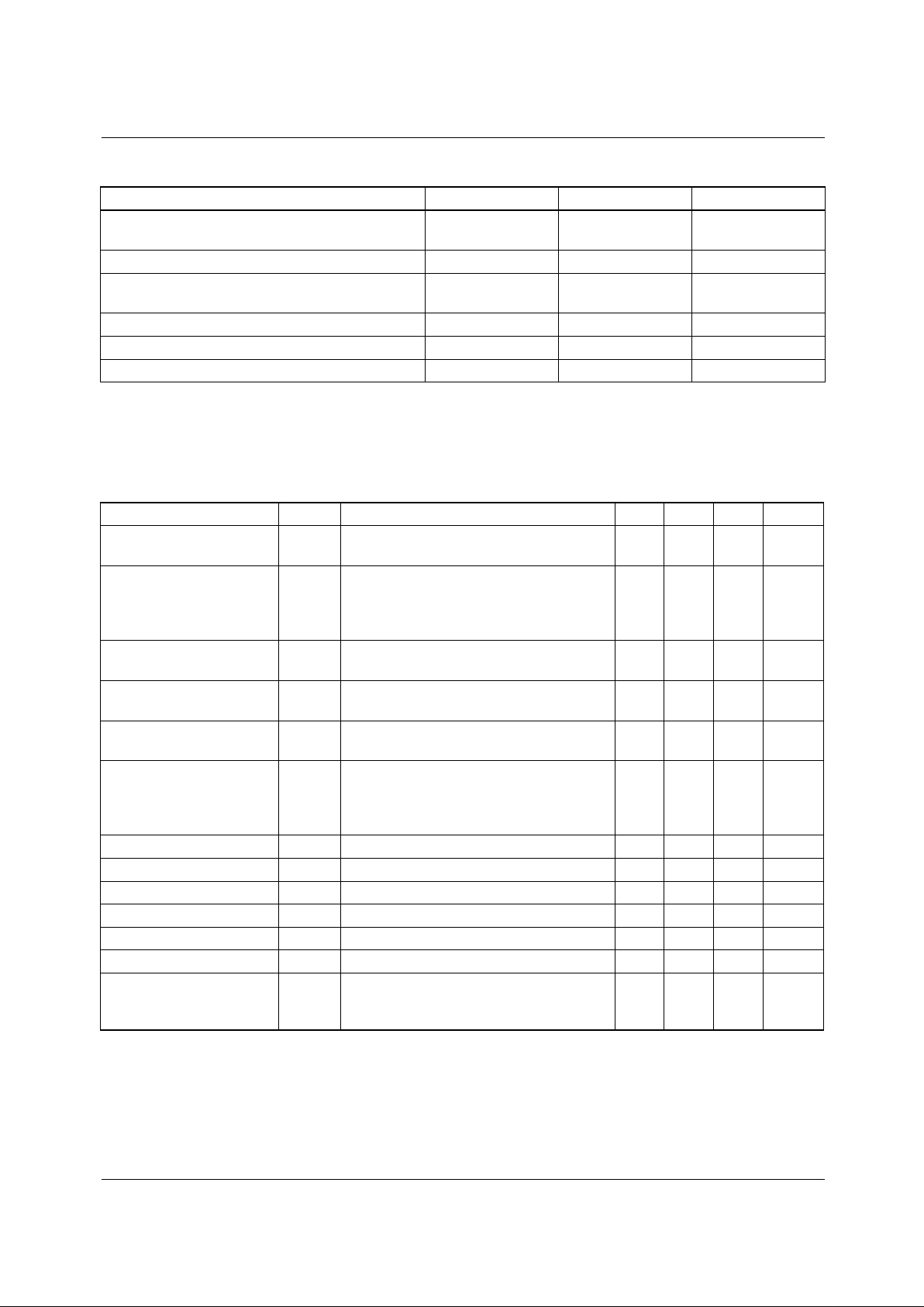
Absolute Maximum Ratings
Electrical Characteristics(KA78T05)
(VI = 10V, IO = 3.0 A, 0 °C ≤ T
J
≤ +125 °C, Po ≤ P
MAX
, unless otherwise specified.)
Note:
1. Load and line regulation are specified at constant junction temperature. Change in Vo due heating effects must be taken into
account separately. Pulse testing with low duty is used .( P
MAX
= 25W)
Parameter Symbol Value Unit
Input Voltage (for V
O
= 5V to 12V)
(for V
O
= 15V)
V
I
35
40
V
V
Power Dissipation PD Internally limited Thermal Resistance, Junction to Air
Tc = +25
°C
RθJA 65 °C/W
Thermal Resistance ,Junction to Case RθJC 2.5 °C/W
Operating Junction Temperature Range T
J
0 ~ +150 °C
Storage Temperature Range T
STG
-65 ~ +150 °C
Parameter Symbol Conditions Min. Typ. Max. Unit
Output Voltage Vo
5mA ≤≤≤≤ Io ≤≤≤≤ 3.0A , T
J
= +25 °C
7.3V ≤≤≤≤ VI ≤≤≤≤ 20V, 5mA ≤≤≤≤ Io ≤≤≤≤ 2.0A
4.8
4.75
5.0
5.0
5.2
5.25
V
Line Regulation (Note1) ∆V
O
7.2V ≤≤≤≤ VI ≤≤≤≤ 35V , Io=5mA, TJ =+25 °C
7.2V ≤≤≤≤ VI ≤≤≤≤ 35V , Io=1.0A, T
J
= +25 °C
7.5V ≤≤≤≤ VI ≤≤≤≤ 20V, Io =2.0A
8.0V ≤≤≤≤ VI ≤≤≤≤ 12V, Io =3.0A
-3.02.5mV
Load Regulation (Note1) ∆V
O
5mA ≤ Io ≤ 3.0A , TJ = +25 °C
5mA ≤ Io ≤ 3.0A
-
10
15
30
80
mV
mV
Thermal Regulation
REG
T
Pulse =10ms, P = 20W
TA = +25 °C
- 0.002 0.03 %Vo/W
Quiescent Current I
Q
5mA ≤ Io ≤ 3.0A , TJ = +25 °C
5mA ≤ Io ≤ 3.0A
-
3.5
4.0
5.0
6.0
mA
mA
Quiescent Current
Change
∆I
Q
7.2V ≤ VI ≤ 35V, Io = 5mA
T
J
= +25 °C ;
7.5V ≤ VI ≤ 20V, Io =2.0A ;
5mA ≤ Io ≤ 3.0A
-0.10.8mA
Ripple Rejection RR f = 120Hz, 8V ≤ V
I
≤ 18V, Io = 2.0A - 75 - dB
Dropout Voltage V
D
Io = 3A ,TJ = +25
°C-2.22.5V
Output Noise Voltage V
N
TA = +25
°C, 10Hz ≤ f ≤ 100KHz - 10 - µV/Vo
Peak Output Current I
PK
TA = +25
°C-5.0-A
Output Resistance Ro f = 1.0kHz - 2.0 - m Ω
Short Circuit Current Limit Isc VI = 35V, T
J
=+25
°C-1.52.5A
Average Temperature
Coefficient of Output
Voltage
∆V
O
/∆T Io = 5.0mA - 0.2 - mV/°C

KA78TXX
3
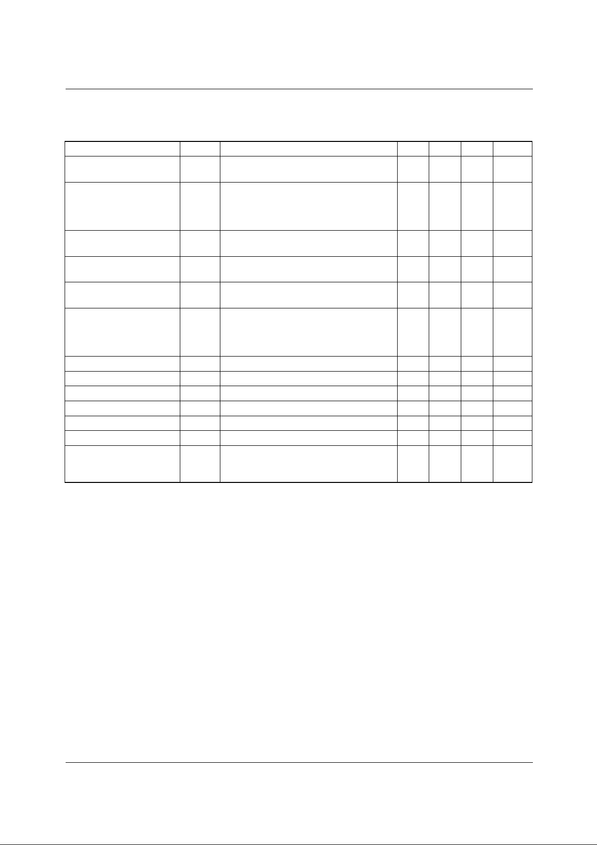
Electrical Characteristics(KA78T12)
(VI = 19V, IO = 3.0 A, 0 °C ≤ T
J
≤ +125 °C, Po ≤ P
MAX
, unless otherwise specified.)
Note:
1. Load and line regulation are specified at constant junction temperature. Change in Vo due heating effects must be taken into
account separately. Pulse testing with low duty is used. ( P
MAX
= 25W)
Parameter Symbol Conditions Min. Typ. Max. Unit
Output Voltage Vo
5mA ≤ Io ≤ 3.0A , T
J
=+25 °C
14.5V ≤ VI ≤ 27V, 5mA ≤ Io ≤ 2.0A
11.5
11.41212
12.5
12.8
V
Line Regulation (Note1) ∆V
O
14.5V ≤ VI ≤ 35V , Io=5mA, TJ =+25 °C
14.5V ≤ VI ≤ 35V , Io=1.0A, T
J
=+25 °C
14.9V ≤ VI ≤ 28V, Io =2.0A
16V ≤ VI ≤ 22V, Io =3.0A
-6.045mV
Load Regulation (Note1) ∆V
O
5mA ≤ Io ≤ 3.0A , TJ =+25 °C
5mA ≤ Io ≤ 3.0A
-
10
15
30
80
mV
mV
Thermal Regulation
REG
T
Pulse =10ms, P = 20W
TA = +25 °C
- 0.002 0.03 %Vo/W
Quiescent Current I
Q
5mA ≤ Io ≤ 3.0A , TJ =+25 °C
5mA ≤ Io ≤ 3.0A
-
3.5
4.0
5.0
6.0
mA
mA
Quiescent Current
Change
∆I
Q
14.5V ≤ VI ≤ 35V, Io = 5mA
T
J
=+25 °C ;
14.9V ≤ VI ≤ 27V, Io =2.0A ;
5mA ≤ Io ≤ 3.0A
-0.10.8mA
Ripple Rejection RR f = 120Hz, 15V ≤ V
I
≤ 25V, Io = 2.0A 57 67 - dB
Dropout Voltage V
D
Io = 3A ,TJ =+25
°C-2.22.5V
Output Noise Voltage V
N
TA =+25
°C, 10Hz ≤ f ≤ 100KHz - 10 - µV/Vo
Peak Output Current I
PK
TA =+25
°C-5.0-A
Output Resistance Ro f = 1.0kHz - 2.0 - mΩ
Short Circuit Current Limit Isc VI = 35V, T
J
=+25
°C-1.52.5A
Average Temperature
Coefficient of Output
Voltage
∆V
O
/∆T Io = 5.0mA - 0.5 - mV/°C
 Loading...