Fairchild Semiconductor KA78RH33R Datasheet

©2001 Fairchild Semiconductor Corporation
www.fairchildsemi.com
Rev. 1.0.1
Features
• Fixed Output Voltage of +3.3V
• Space Saving SMD types of DPAK
• 1V(Typ) Dropout at Io=800mA
• Output Current of 800mA
• Thermal Shutdown Protection
• Over Current Protection
• Output trimmed to +/-1% Tolerance
• No minimum Load Requ i re m en t
Description
The KA78RH33 i s a +3.3V fixed Low Dropout Voltage
Regulator specifically designed for use in low voltage operation. The maximum load current is 0.8A and the dropout
voltage is guaranteed to be 1V(Typ). The Dropout Voltage
varies with load current. The regulator consists of composite PNP-NPN pass transistors.
D-PAK
1. GND 2. Vout 3.Vin
1
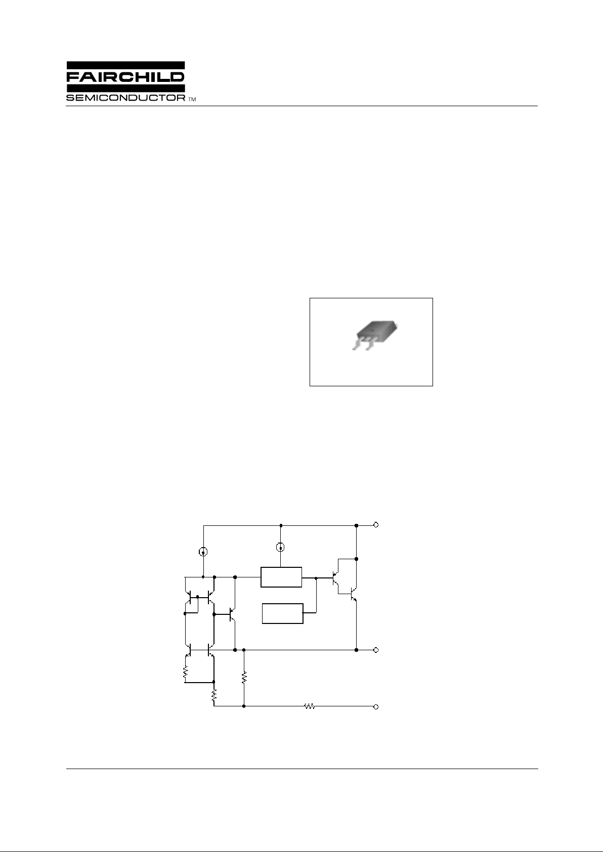
Internal Block Diagram
3.Vin
2.Vout
1.GND
CURRENT
GENERATOR
PROTECTION
CIRCUIT
KA78RH33
Semi Low Dropout Voltage Regulator

KA78RH33
2
Absolute Maximum Ratings
Temperature Characteristics
Electrical Characteristics
(Refer to the test circuit. Vin= 5V, Co=10uF, Ta = 25°C, unless otherwise specified.)
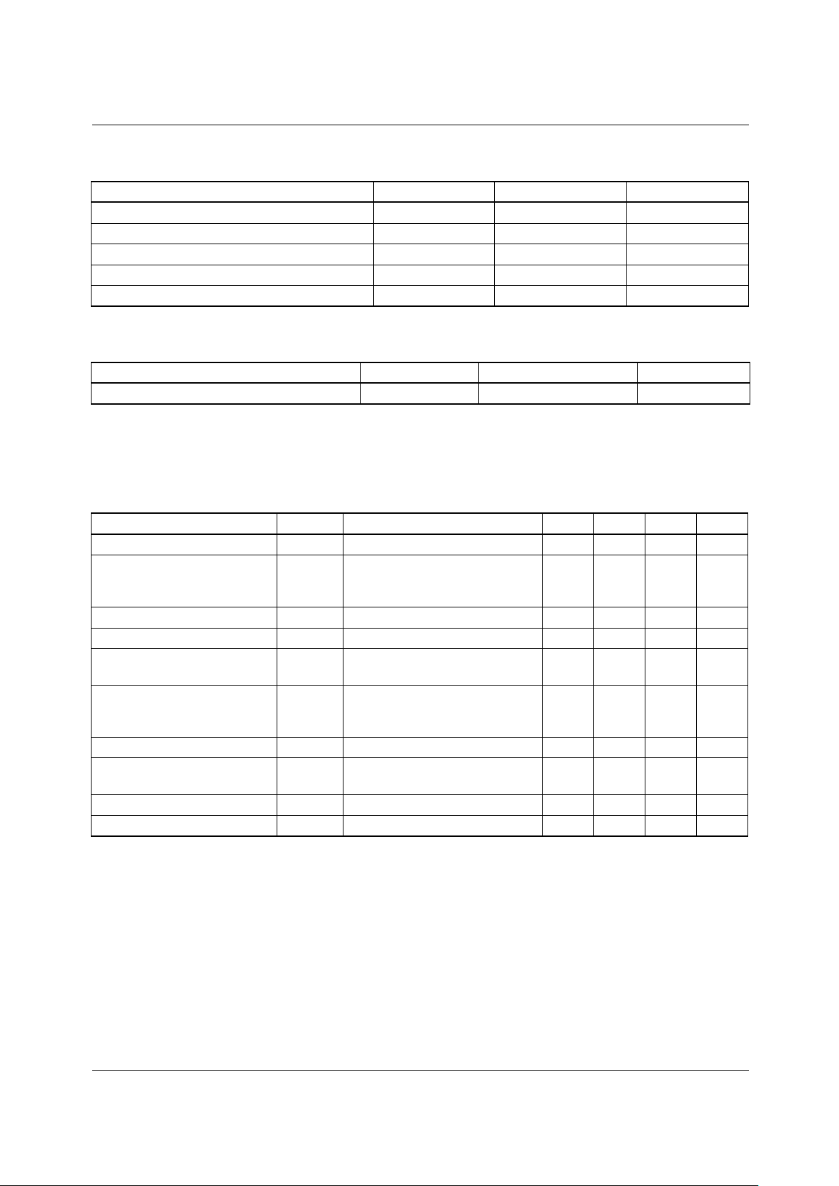
Parameter Symbol Value Unit
Power Supply Input Voltage Vin 15 V
Output Load Current Io 800 mA
Junction Temperature Tj 150 °C
Operating Junction Temperature Topr -25 ~ 125 °C
Storage Temperature Tstg -55 ~ 150 °C
Parameter Symbol Value Unit
Temperature Coefficient of Output Voltage △ Vo/ △ T + / -0.02 % / °C
Parameter Symbol Conditions Min. Typ. Max. Unit
Output Voltage Vout Io=10mA, Tj=25°C 3.27 3.3 3.33 V
Output Voltage Vout
Vin = 4.8V to 12V
Io = 10mA to 800mA
Tj = -25°C to 125°C
3.23 3.3 3.37 V
Line Regulation Rline Vin=4.8V to 12V, Io=10mA - 1 10 mV
Load Regulation Rload Io = 10mA to 800mA - 1 20 mV
Ripple Rejection RR
f=120Hz, Io=500mA
Vin = 6.3 +/- 1Vrms
55 - - dB
Dropout Voltage Vdrop
Io = 100mA
Io = 500mA
Io = 800mA
-
-
-
1
1.05
1.1
1.2
1.25
1.4
V
Quiescent Current Iq Vin <= 12V - 5 10 mA
Temperature Coefficient of
Output Voltage
△ Vo/ △ T
Tj = -25°C to 125°C
Io = 10mA
-0.2-mV/°C
Peak Output Current Ipk Vin = 6.3V 800 - - mA
Output Noise Voltage Vn f = 10Hz to 10KHz - 100 - µVrms
 Loading...