

Fairchild Semiconductor ISL9N7030BLS3ST, ISL9N7030BLP3 Datasheet
E
Data Sheet January2002
30V, 0.009 Ohm, 75A, N-Channel Logic
Level UltraFET® Trench Power MOSFETs
This devi ce em ploys a new advanced trench MO SFET
technology and features low gate charge while maintaining
low on-resistance.
Optimized for switching ap plications, this device improves
the overa ll effi ci enc y of DC/D C converters and allows
operation to higher switching frequencies.
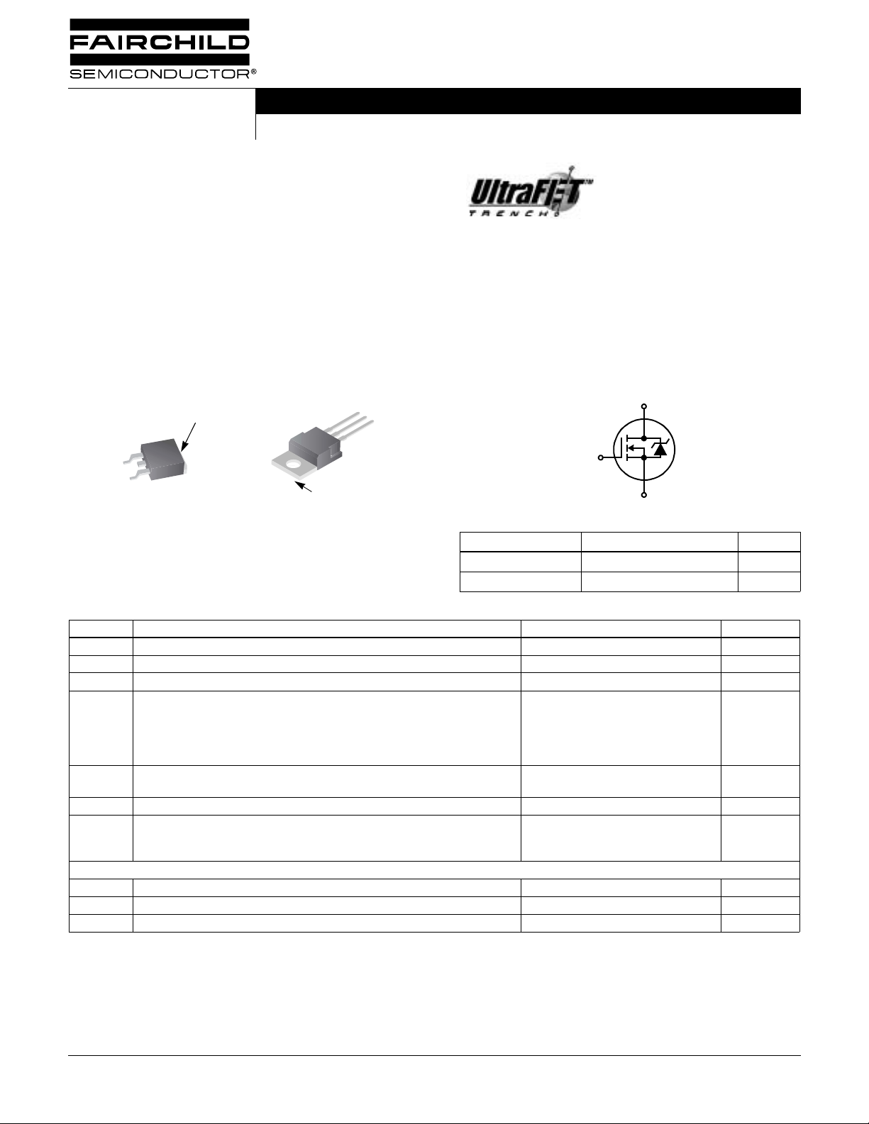
Packaging
ISL9N7030BLS3ST
JEDEC TO-263AB
DRAIN
(FLANGE)
ISL9N7030BLP3
JEDEC TO-220AB
SOURCE
DRAIN
GAT
ISL9N7030BLP3, ISL9N7030BLS3ST
PWM
Optimized
Features
•Fast Switching
•r
•r
•Qg Total 24nC (Typ), VGS = 5V
•Q
•C
Symbol
= 0.0064Ω (Typ), V
DS(ON)
= 0.010Ω (Typ), V
DS(ON)
(Typ) . . . . . . . . . . . . . . . . . . . . . . . . . . . . . . . . . .11nC
gd
(Typ) . . . . . . . . . . . . . . . . . . . . . . . . . . . . . . . 2600pF
ISS
GS
GS
= 10V
= 4.5V
D
G
GATE
SOURCE
DRAIN
(FLANGE)
S
Ordering Information
PART NUMBER PACKAGE BRAND
ISL9N7030BLP3 TO-220AB 7030BL
ISL9N7030BLS3ST TO-263AB (Tape and Reel) 7030BL
Absolute Maximum Ratings
SYMBOL PARAMETER ISL9N7030BLP3, I SL9N703 0BLS3ST UNITS
V
DSS
V
DGR
V
I
DM
P
, T
T
J
T
T
THERMAL SPECIFICATIONS
R
R
R
NOTE:
1. T
CAUTION: Stresses above those listed in “Absolute Maximum Ratings” may cause permanent damage to the device. This is a stress only rating and operation of the
device at these or any other conditions above those indicated in the operational sections of this specification is not implied.
All Fairchild semiconductor products are manufactured, assembled and tested under ISO9000 and QS9000 quality systems certification.
Drain to Source Voltage (Note 1) 30 V
Drain to Gate Voltage (RGS = 20kΩ) (Note 1) 30 V
Gate to Source Voltage ±20 V
GS
Drain Current
I
D
I
D
I
D
D
STG
L
pkg
θJC
θJA
θJA
= 25oC to 150oC.
J
Continuous (T
Continuous (T
Continuous (T
Pulsed Drain Current
Power Dissipation
Derate Above 25
Operating and Storage Temperature -55 to 175
Maximum Temperature for Soldering
Leads at 0.063in (1.6mm) from Case for 10s
Package Body for 10s, See T e chbrief TB334
Thermal Resistance Junction to Case, TO-220, TO-263 1.5
Thermal Resistance Junction to Ambient, TO-220, TO-263 62
Thermal Resistance Junction to Ambient, TO-263, 1in2 copper pad area 43
Product reliability information can be found at http://www.fairchildsemi.com/products/discrete/reliability/index.html
C
C
C
TC = 25oC, Unless Otherwise Specified
= 25oC, VGS = 10V) (Figure 2)
= 100oC, VGS = 4.5V) (Figure 2)
= 25oC, VGS = 10V, R
o
C
For severe environments, see our Automotive products.
= 43oC/W)
θJA
75
48
15
Figure 4
100
0.67
300
260
A
A
A
A
W
W/oC
o
C
o
C
o
C
o
C/W
o
C/W
o
C/W
©2002 Fairchild Semiconductor Corpo ration ISL9N7030BLP3, ISL9N7030BLS3ST Rev. B
ISL9N7030BLP3, ISL9N703 0BLS3ST
Electrical Specifications
TC = 25oC, Unless Otherwise Specified
PARAMETER SYMBOL TEST CONDITIONS MIN TYP MAX UNITS
OFF STATE SPECIFICATIONS
Drain to Source Breakdown Voltage BV
Zero Gate Voltage Drain Current I
Gate to Source Leakage Current I
ON STATE SPECIFICATIONS
Gate to Source Threshold Voltage V
Drain to Source On Resistance r
SWITCHING SPECIFICATIONS (V
GS
= 4.5V)
Turn-On Time t
Turn-On Delay Time t
Rise Time t
Turn-Off Delay Time t
Fall Time t
Turn-Off Time t
SWITCHING SPECIFICATIONS (V
GS
= 10V)
Turn-On Time t
Turn-On Delay Time t
Rise Time t
Turn-Off Delay Time t
Fall Time t
Turn-Off Time t
GATE CHARGE SPECIFICATIONS
Total Gate Charge at 10V Q
Total Gate Charge at 5V Q
Threshold Gate Charge Q
Gate to Source Gate Charge Q
Gate to Drain “Miller” Charge Q
CAPACITANCE SPECIFICATIONS
Input Capacitance C
Output Capacitance C
Reverse Transfer Capacitance C
DSSID
DSS
VDS = 25V, VGS = 0V - - 1 µA
V
GSS
GS(TH)VGS
DS(ON)ID
ON
VGS = ±20V - - ±100 nA
I
D
VDD = 15V, ID = 15A
V
d(ON)
d(OFF)
OFF
ON
d(ON)
d(OFF)
OFF
g(TOT)VGS
g(5)
g(TH)
ISS
OSS
RSS
(Figures 13, 17, 18)
r
f
VDD = 15V, ID = 15A,
V
(Figures 14, 17, 18)
r
f
VGS = 0V to 5V - 24 37 nC
VGS = 0V to 1V - 2.6 4.0 nC
gs
gd
VDS = 15V, VGS = 0V,
f = 1MHz
(Figure 11)
= 250µA, VGS = 0V (Figure 10) 30 - - V
= 25V, VGS = 0V, TC = 150oC - - 250 µA
DS
= VDS, ID = 250µA (Figure 9 1 - 3 V
= 75A, VGS = 10V (Figures 7, 8) - 0.007 0.009 Ω
= 48A, VGS = 4.5V (Figure 7) - 0.010 0.012 Ω
- - 122 ns
= 4.5V, RGS = 6.2Ω
GS
-15-ns
-67-ns
-35-ns
-32-ns
- - 100 ns
- - 71 ns
= 10V, R
GS
GS
= 6.2Ω,
-8-ns
-40-ns
-64-ns
-31-ns
- - 142 ns
= 0V to 10V VDD = 15V,
I
= 48A,
D
= 1.0mA
I
g(REF)
(Figures 12, 15, 16)
-4568nC
-7-nC
-8-nC
- 2600 - pF
- 520 - pF
- 225 - pF
Source to Drain Diode Specifications
PARAMETER SYMBOL TEST CONDITIONS MIN TYP MAX UNITS
I
Source to Drain Diode Voltage V
Reverse Recovery Time t
Reverse Recovered Charge Q
©2002 Fairchild Semiconductor Corpo ration ISL9N7030BLP3, ISL9N7030BLS3ST Rev. B
SD
rr
RR
= 48A - - 1.25 V
SD
= 20A - - 1.0 V
I
SD
ISD = 48A, dISD/dt = 100A/µs--26ns
ISD = 48A, dISD/dt = 100A/µs--14nC
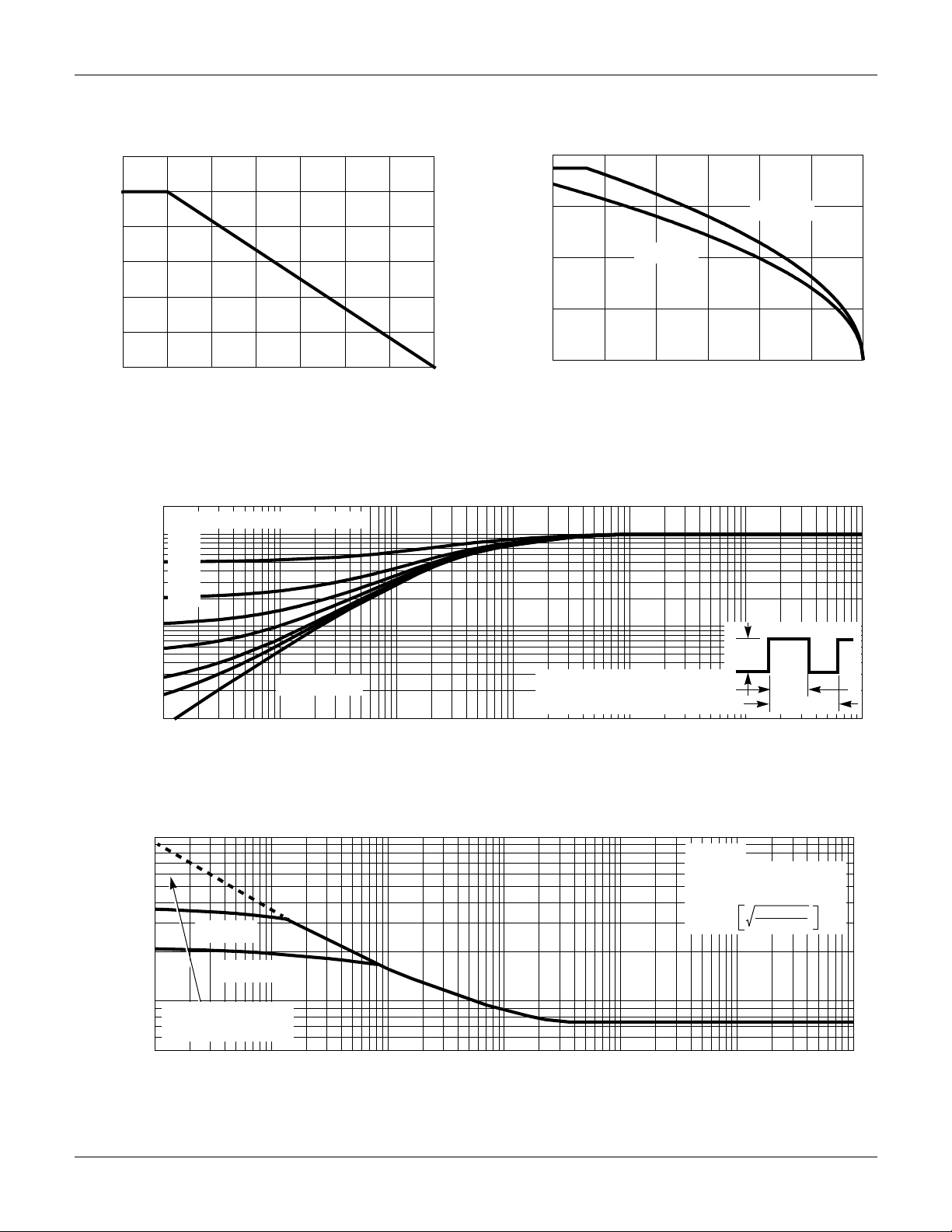
Typical Performance Curves
5
ISL9N7030BLP3, ISL9N703 0BLS3ST
1.2
1.0
0.8
0.6
0.4
0.2
POWER DISSIPATION MULTIPLIER
0
0 25 50 75 100 175
125
150
TC, CASE TEMPERATURE (oC)
FIGURE 1. NORMALIZED POWER DISSIPATI ON vs CASE
TEMPERATURE
2
DUTY CYCLE - DESCENDING ORDER
0.5
1
0.2
0.1
0.05
0.02
0.01
80
60
40
, DRAIN CURRENT (A)
20
D
I
0
25 50 75 100 125 150 17
VGS = 4.5V
VGS = 10V
TC, CASE TEMPERATURE (oC)
FIGURE 2. MAXIMUM CONTINUOUS DRAIN CURRENT vs
CASE TEMPERATURE
, NORMALIZED
Z
0.1
+ T
P
DM
t
1
t
C
0
10
2
1
10
θJC
THERMAL IMPEDANCE
0.01
SINGLE PULSE
-5
10
-4
10
-3
10
NOTES:
DUTY FACTOR: D = t
PEAK TJ = PDM x Z
-2
10
1/t2
x R
θJC
θJC
-1
10
t, RECTANGULAR PULSE DURATION (s)
FIGURE 3. NORMALIZED MAXIMUM TRANSIENT THERMAL IMPEDANCE
, PEAK CURRENT (A)
I
DM
1000
100
TRANSCONDUCTANCE
MAY LIMIT CURRENT
IN THIS REGION
50
-5
10
VGS = 10V
VGS = 5V
-4
10
-3
10
-2
10
-1
10
t, PULSE WIDTH (s)
TC = 25oC
FOR TEMPERATURES
ABOVE 25
o
C DERATE PEAK
CURRENT AS FOLLOWS:
175 - T
I = I
25
0
10
150
C
1
10
FIGURE 4. PEAK CURRENT CAPABILITY
©2002 Fairchild Semiconductor Corpo ration ISL9N7030BLP3, ISL9N7030BLS3ST Rev. B
 Loading...