

Fairchild Semiconductor ISL9N307AD3ST Datasheet
February 2002
ISL9N307AD3ST
N-Channel Logic Level PWM Optimized UltraFET® Trench Power MOSFETs
ISL9N307AD3ST
General Description
This device employs a new advanced trench MOSFET
technology and features low gate charge while maintaining
low on-resistance.
Optimized for switching applications, this device improves
the overall efficiency of DC/DC converters and allows
operation to higher switching frequencies.
Applications
• DC/DC converters
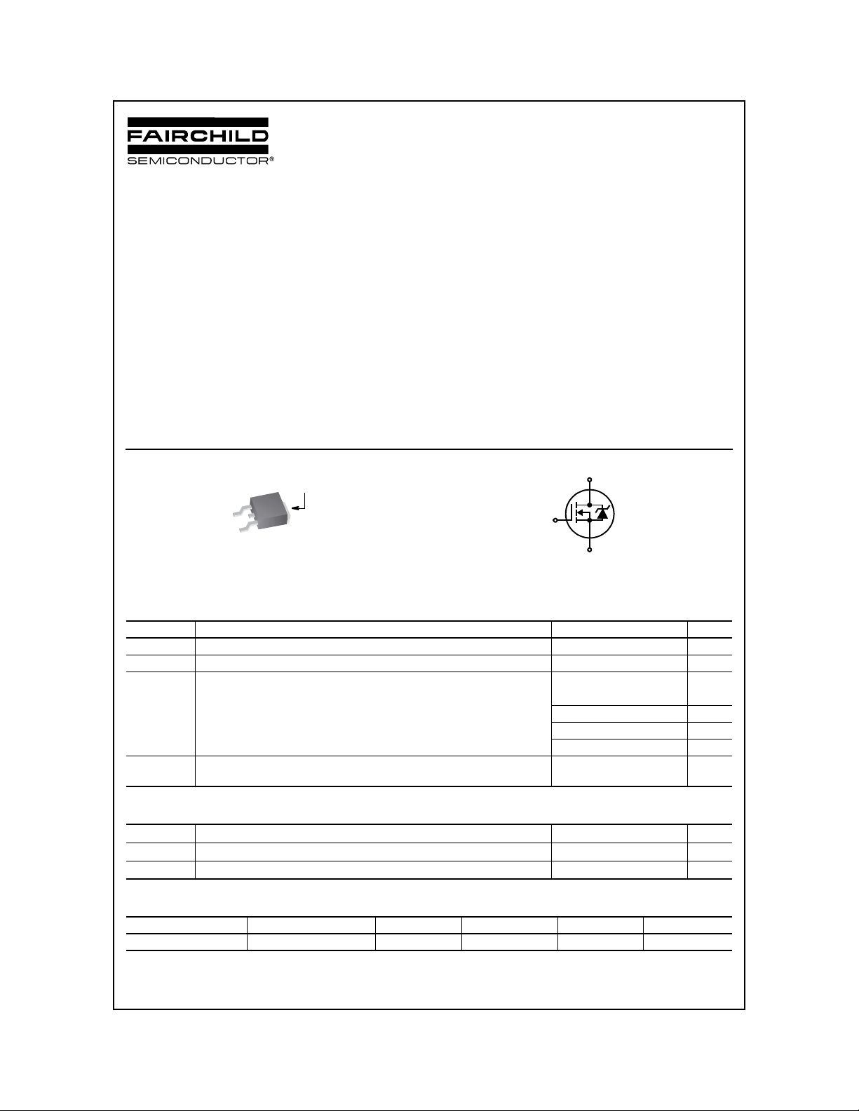
DRAIN (FLANGE)
GATE
SOURCE
Features
• Fast switching
•r
•r
•Q
•Q
•C
= 0.006Ω (Typ), VGS = 10V
DS(ON)
= 0.010Ω (Typ), VGS = 4.5V
DS(ON)
(Typ) = 28nC, VGS = 5V
g
(Typ) = 10nC
gd
(Typ) = 3000pF
ISS
D
G
S
TO-252
MOSFET Maximum Ratings
Symbol Parameter Ratings Units
V
DSS
V
GS
I
D
P
D
Drain to Source Voltage 30 V
Gate to Source Voltage ±20 V
Drain Current
Continuous (T
Continuous (T
Continuous (T
Pulsed Figure 4 A
Power dissipation
Derate above 25
= 25oC, VGS = 10V)
C
= 100oC, VGS = 4.5V) 50 A
C
= 25oC, VGS = 10V, R
C
o
C
TA = 25°C unless otherwise noted
= 52oC/W) 15 A
θJA
50 A
100
0.67
W
W/oC
Thermal Characteristics
R
θJC
R
θJA
R
θJA
Thermal Resistance Junction to Case TO-252 1.36
Thermal Resistance Junction to Ambient TO-252 100
Thermal Resistance Junction to Ambient TO-252, 1in2 copper pad area 52
Package Marking and Ordering Information
Device Marking Device Package Reel Size Tape Width Quantity
N307AD ISL9N307AD3ST TO-252AA 330mm 16mm 2500 units
©2002 Fairchild Semiconductor Corporation
o
C/W
o
C/W
o
C/W
Rev. B, February 2002
ISL9N307AD3ST
Electrical Characteristics
TA = 25°C unless otherwise noted
Symbol Parameter Test Conditions Min Typ Max Units
Off Characteristics
B
I
DSS
I
GSS
VDSS
Drain to Source Breakdown Voltage ID = 250µA, VGS = 0V 30 - - V
V
= 25V - - 1
Zero Gate Voltage Drain Current
DS
= 0V TC = 150
V
GS
o
- - 250
Gate to Source Leakage Current VGS = ±20V - - ±100 nA
On Characteristics
V
GS(TH)
r
DS(ON)
Gate to Source Threshold Voltage VGS = VDS, ID = 250µA1-3V
I
= 50A, VGS = 10V - 0.006 0.007
Drain to Source On Resistance
D
I
= 50A, VGS = 4.5V - 0.010 0.0115
D
Dynamic Characteristics
C
ISS
C
OSS
C
RSS
Q
g(TOT)
Q
g(5)
Q
g(TH)
Q
gs
Q
gd
Input Capacitance
Output Capacitance - 580 - pF
Reverse Transfer Capacitance - 250 - pF
Total Gate Charge at 10V VGS = 0V to 10V
Total Gate Charge at 5V VGS = 0V to 5V - 28 42 nC
Threshold Gate Charge VGS = 0V to 1V - 3.0 4.5 nC
Gate to Source Gate Charge - 11 - nC
Gate to Drain “Miller” Charge - 10 - nC
Switching Characteristics
t
ON
t
d(ON)
t
r
t
d(OFF)
t
f
t
OFF
Turn-On Time
Turn-On Delay Time - 20 - ns
Rise Time - 70 - ns
Turn-Off Delay Time - 40 - ns
Fall Time - 40 - ns
Turn-Off Time - - 120 ns
(VGS = 4.5V)
= 15V, VGS = 0V,
V
DS
f = 1MHz
V
= 15V, ID = 15A
DD
V
= 4.5V, RGS = 5.0Ω
GS
= 15V
V
DD
I
= 50A
D
= 1.0mA
I
g
-3000- pF
-5075nC
- - 135 ns
µA
Ω
Switching Characteristics
t
ON
t
d(ON)
t
r
t
d(OFF)
t
f
t
OFF
Turn-On Time
Turn-On Delay Time - 10 - ns
Rise Time - 45 - ns
Turn-Off Delay Time - 60 - ns
Fall Time - 35 - ns
Turn-Off Time - - 143 ns
(VGS = 10V)
= 15V, ID = 15A
V
DD
= 10V, RGS = 5.0Ω
V
GS
- - 83 ns
Unclamped Inductive Switching
t
AV
Avalanche Time ID = 3.3A, L = 3mH 220 - - µs
Drain-Source Diode Characteristics
I
= 50A - - 1. 25 V
V
SD
t
rr
Q
RR
©2002 Fairchild Semiconductor Corporation Rev. B, February 2002
Source to Drain Diode Voltage
Reverse Recovery Time ISD = 50A, dISD/dt = 100A/µs- - 26 ns
Reverse Recovered Charge ISD = 50A, dISD/dt = 100A/µs- - 13 nC
SD
= 25A - - 1.0 V
I
SD
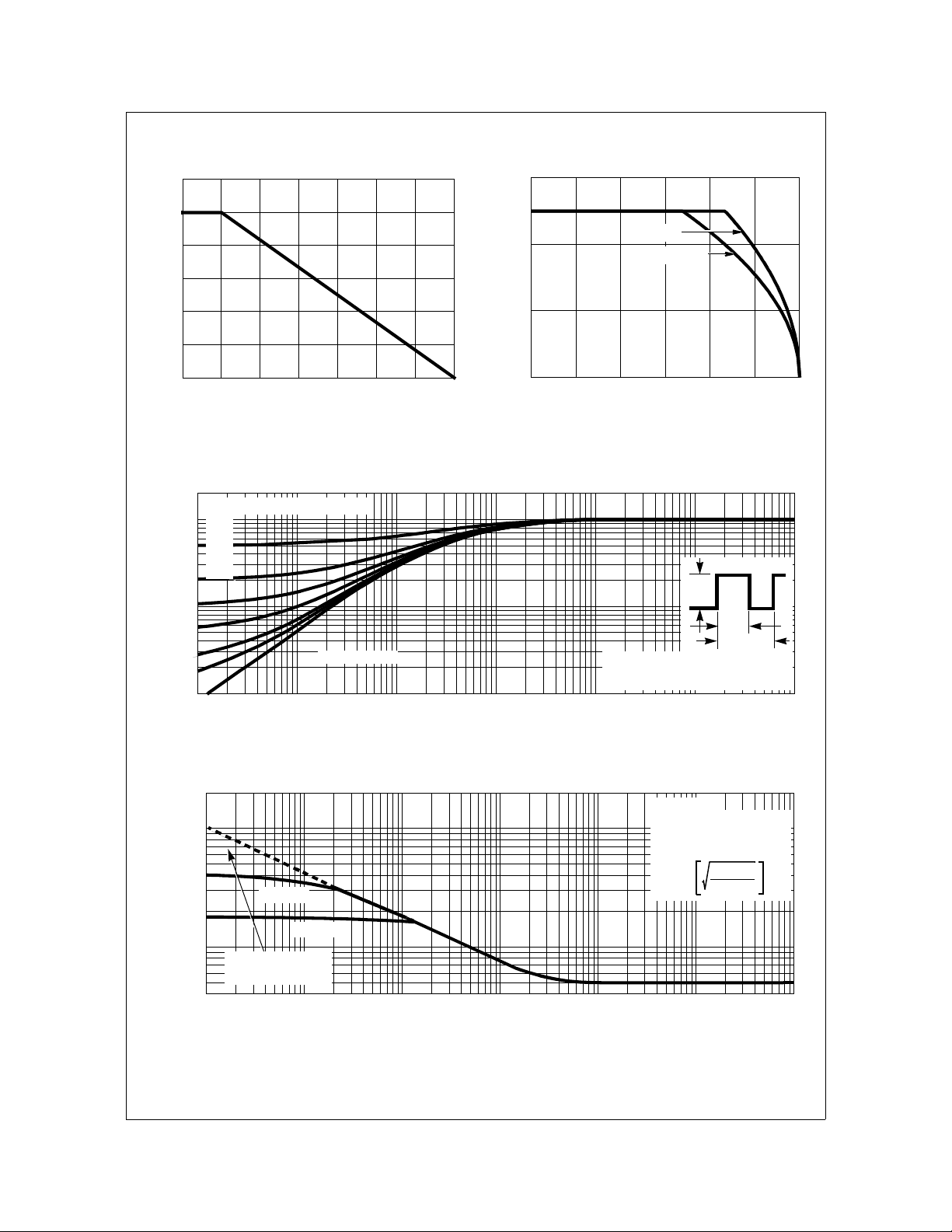
Typical Characteristic
ISL9N307AD3ST
1.2
1.0
0.8
0.6
0.4
0.2
POWER DISSIPATION MULTIPLIER
0
0 25 50 75 100 175
125
150
TC, CASE TEMPERATURE (oC)
Figure 1. Normalized Power Dissipation vs
Ambient Temperature
2
DUTY CYCLE - DESCENDING ORDER
0.5
1
0.2
0.1
0.05
0.02
0.01
0.1
, NORMALIZED
θJC
Z
THERMAL IMPEDANCE
0.01
-5
10
-4
10
SINGLE PULSE
-3
10
t, RECTANGULAR PULSE DURATION (s)
60
V
= 10V
40
20
, DRAIN CURRENT (A)
D
I
GS
V
= 4.5V
GS
0
25 50 75 100 125 150 175
TC, CASE TEMPERATURE (oC)
Figure 2. Maximum Contin uous Drain Current vs
Case Temperature
P
DM
t
1
t
x R
2
2
+ T
θJC
C
1
10
NOTES:
DUTY FACTOR: D = t1/t
PEAK TJ = PDM x Z
-2
10
-1
10
θJC
10
0
Figure 3. Normalized Maximum Transient Thermal Impedance
2000
1000
VGS = 10V
, PEAK CURRENT (A)
DM
I
100
TRANSCONDUCTANCE
MAY LIMIT CURRENT
IN THIS REGION
40
-5
10
VGS = 5V
-4
10
-3
10
-2
10
-1
10
t, PULSE WIDTH (s)
TC = 25oC
FOR TEMPERATURES
ABOVE 25oC DERATE PEAK
CURRENT AS FOLLOWS:
175 - T
I = I
25
10
C
150
0
1
10
Figure 4. Peak Current Capability
©2002 Fairchild Semiconductor Corporation Rev. B, February 2002
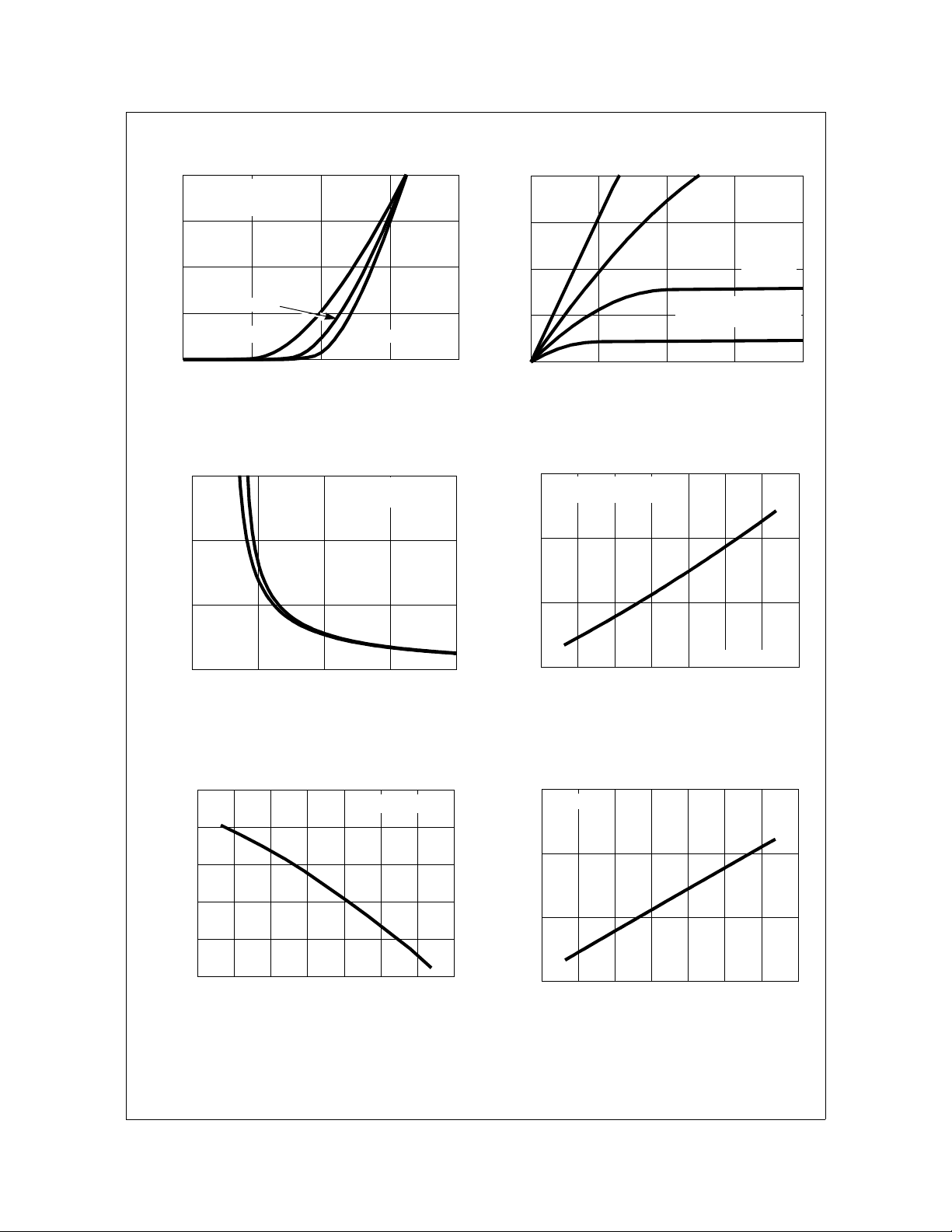
ISL9N307AD3ST
Typical Characteristic
100
PULSE DURATION = 80µs
DUTY CYCLE = 0.5% MAX
V
= 15V
DD
75
50
25
, DRAIN CURRENT (A)
D
I
0
TJ = 25oC
TJ = 175oC
12345
VGS, GATE TO SOURCE VOLTAGE (V)
(Continued)
TJ = -55oC
Figure 5. Transfer Ch aracteri stics Figure 6. Saturation Characteristics
20
15
ID = 28A
ID = 50A
PULSE DURATION = 80µs
DUTY CYCLE = 0.5% MAX
100
TC = 25oC
VGS = 10V
75
50
25
, DRAIN CURRENT (A)
D
I
0
00.511.52
VDS, DRAIN TO SOURCE VOLTAGE (V)
2.0
PULSE DURATION = 80µs
DUTY CYCLE = 0.5% MAX
1.5
VGS = 4.5V
VGS = 3.5V
PULSE DURATION = 80µs
DUTY CYCLE = 0.5% MAX
VGS = 3V
10
, DRAIN TO SOURCE
ON RESISTANCE (mΩ)
DS(ON)
r
5
246810
VGS, GATE TO SOURCE VOLTAGE (V)
Figure 7. Drain to Source On Resis tanc e vs Ga te
Voltage and Drain Current
1.4
1.2
1.0
0.8
0.6
NORMALIZED GATE
THRESHOLD VOLTAGE
0.4
-80 -40 0 40 80 120 160 200
TJ, JUNCTION TEMPERATURE (oC)
VGS = VDS, ID = 250µA
Figure 9. Normalized Gate Thres hold Volta ge v s
Junction Temperature
1.0
ON RESISTANCE
NORMALIZED DRAIN TO SOURCE
0.5
-80 -40 0 40 80 120 160 200
TJ, JUNCTION TEMPERATURE (oC)
VGS = 10V, ID =50A
Figure 8. Normalized Drain to Source On
Resistance vs Junction Temperature
1.2
ID = 250µA
1.1
1.0
BREAKDOWN VOLTAGE
NORMALIZED DRAIN TO SOURCE
0.9
-80 -40 0 40 80 120 160 200
TJ, JUNCTION TEMPERATURE (oC)
Figure 10. Normalized Drain to Source
Breakdown Voltage vs Junction Temp er atu re
©2002 Fairchild Semiconductor Corporation Rev. B, February 2002
 Loading...