

Fairchild Semiconductor HGTG30N60B3D Datasheet
HGTG30N60B3D, HGT4E30N60B3DS
Data Sheet Decemb er 2001
60A, 600V, UFS Series N-Channel IGBT
with Anti-Parallel Hyperfast Diode
The HGTG30N60B3D, and HGT4E30N60B3DS are MOS
gated high voltage switching devices combining the best
featuresof MOSFETs and bipolar transistors.These devices
have t he high input impedance of a MOSFET and t he low
on-stateconduction loss of a bipolar transistor. The much
lower on-state voltage dr op varies only moderately between
o
25
C and 150oC. The IGBT used is the development type
TA49170. The diode used in anti-parallel with the IGBT is the
development type TA49053.
The IGBT is ideal f or many high voltageswitching
applicationsoperating at moderate frequencies where low
conductionlosses are essential, such as: AC and DC motor
controls, power supplies and drivers for solenoids, relays
and contactors.
Formerly Developmental TypeTA49172.
Ordering Information
PART NUMBER PACKAGE BRAND
HGTG30N60B3D TO-247 G30N60B3D
HGT4E30N60B3DS TO-268AA G30N60B3D
NOTE: When ordering, use the entire part number.
Packaging
Symbol
JEDEC STYLE TO-247
TO-268AA
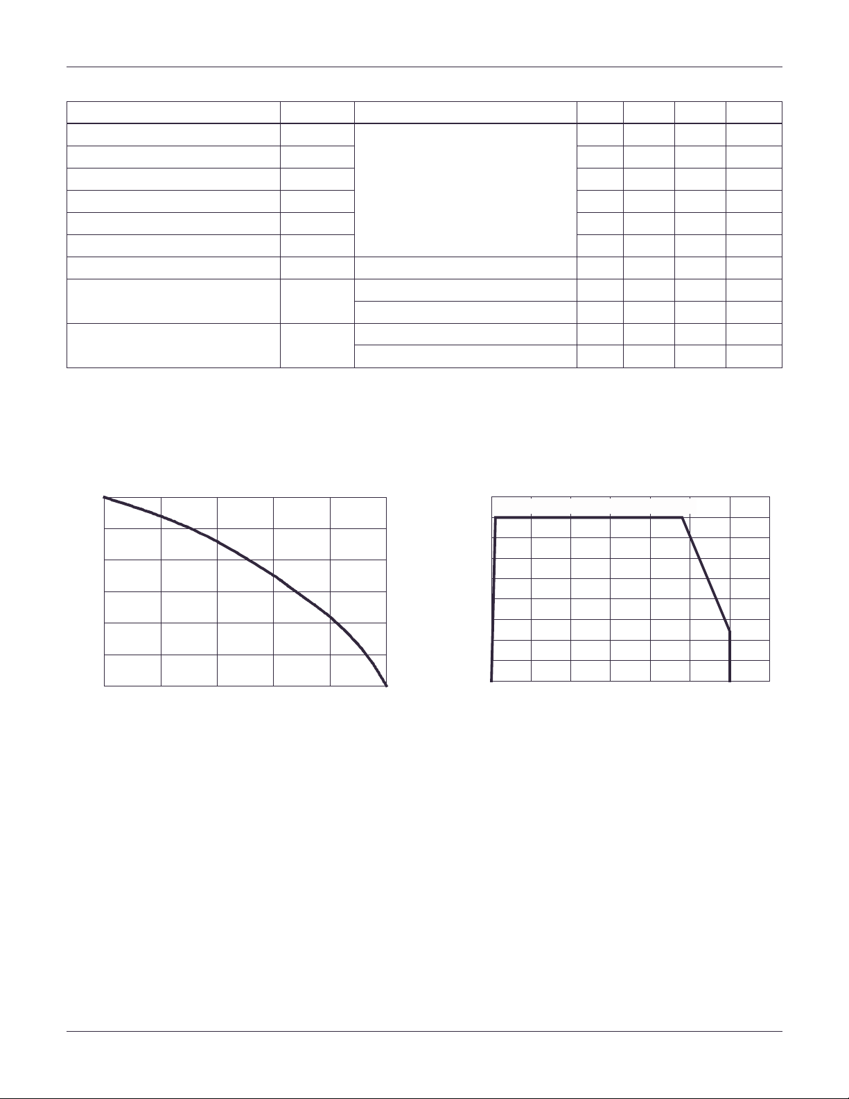
G
E
C
E
C
G
C
Features
• 60A, 600V, TC=25oC
• 600V Switching SOA Capability
• TypicalFallTime.................90nsatT
=150oC
J
• Short Circuit Rating
• Low Conduction Loss
• Hyperfast Anti-Parallel Di ode
FAIRCHILD CORPORATION I GB T PRODUCT IS COVERED BY ONE OR MORE OF THE FOLLOWING U.S. PATENTS
4,364,073 4,417,385 4,430,792 4,443,931 4,466,176 4,516,143 4,532,534 4,587,713
4,598,461 4,605,948 4,620,211 4,631,564 4,639,754 4,639,762 4,641,162 4,644,637
4,682,195 4,684,413 4,694,313 4,717,679 4,743,952 4,783,690 4,794,432 4,801,986
4,803,533 4,809,045 4,809,047 4,810,665 4,823,176 4,837,606 4,860,080 4,883,767
4,888,627 4,890,143 4,901,127 4,904,609 4,933,740 4,963,951 4,969,027
G
E
©2001 Fairchild SemiconductorCorporation HGTG30N60B3D,HGT4E30N60B3DS Rev. B1
HG TG30N60B3D, HGT4E30N60B3DS
Absolute Maxim um Ratings T
=25oC, Unless Otherwise Specified
C
HGTG30N60B3D,
HGT4E30N60B3DS UNITS
CollectortoEmitterVoltage..............................................BV
CES
600 V
Collector Current Continuous
=25oC.........................................................I
At T
C
At T
=110oC.......................................................I
C
Average Diode Forward Currentat 110
o
C.................................I
CollectorCurrentPulsed(Note1)...........................................I
GatetoEmitterVoltageContinuous.........................................V
GatetoEmitterVoltagePulsed...........................................V
Switching Safe Operating Area at T
Power Dissipation Total at T
C
Power Dissipation Derating T
=150oC(Figure2)....................... SSOA 60Aat600V
J
=25oC.........................................P
>25oC.......................................... 1.67 W/oC
C
OperatingandStorageJunctionTemperatureRange........................T
MaximumLeadTemperatureforSoldering.....................................T
Short CircuitWithstand Time (Note 2) at V
Short CircuitWithstand Time (Note 2) at V
CAUTION: Stresses above those listed in “Absolute Maximum Ratings” may cause permanent damage to the device. This is a stress only rating and operationofthe
device at these or any other conditions above those indicated in the operational sections of this specification is not implied.
=12V..............................t
GE
=10V..............................t
GE
C25
C110
EC(AVG)
CM
GES
GEM
D
J,TSTG
L
SC
SC
60 A
30 A
25 A
220 A
±20 V
±30 V
208 W
-55to150
260
4 µs
10 µs
o
C
o
C
NOTES:
1. Pulse width limitedby maximum junctiontemperature.
2. V
=360V,TJ= 125oC, RG=3Ω.
CE(PK)
Electrical Specifications T
=25oC, Unless Otherwis e Specified
C
PARAMETER SYMBOL TEST CONDITIONS MIN TYP MAX UNITS
Collector to Emitter Breakdown Voltage BV
Collector to Emitter Leakage Current I
Collector to Emitter Saturation Voltage V
Gate to Emitter Threshold Voltage V
Gate to Emitter Leakage Current I
CESIC
CES
CE(SAT)IC=IC110
GE(TH)IC
GES
Switching SOA SSOA T
Gate to Emitter Plateau Voltage V
On-State Gate Charge Q
Current Turn-On Delay Time t
Current Rise Time t
Current Turn-Off Delay Time t
Current Fall Time t
Turn-On Energy E
Turn-Off Energy (Note 3) E
GEP
G(ON)IC=IC110
d(ON)I
rI
d(OFF)I
fI
ON
OFF
=250µA, VGE=0V 600 - - V
VCE=BV
CES
,
V
=15V
GE
=250µA, VCE=V
TC=25oC - - 250 µA
=150oC--3mA
T
C
=25oC - 1.45 1.9 V
T
C
T
=150oC-1.72.1V
C
GE
4.2 5 6 V
VGE= ±20V - - ±250 nA
=150oC, RG=3Ω,
J
V
=15V,L=100µH
GE
IC=I
C110,VCE
,
V
=0.5BV
CE
CES
=0.5BV
V
V
CES
VGE= 15V - 170 190 nC
V
IGBT and Diode at TJ=25oC,
I
CE=IC110
V
CE
V
GE
R
G
L=1mH,
=0.8BV
=15V,
=3Ω,
,
,
CES
Test Circuit (Figure 19)
= 480V 200 - - A
CE (PK)
=600V 60 - - A
CE (PK)
-7.2- V
= 20V - 230 250 nC
GE
-36- ns
-25- ns
-137 - ns
-58- ns
- 550 800 µJ
- 680 900 µJ
©2001 Fairchild S emiconductor Corporation HGTG30N60B3D,HGT4E30N60B3DS Rev. B 1
HG TG30N60B3D, HGT4E30N60B3DS
Electrical Specifications T
=25oC, Unless Otherwis e Specified (Continued)
C
PARAMETER SYMBOL TEST CONDITIONS MIN TYP MAX UNITS
Current Turn-On Delay Time t
d(ON)I
Current Rise Time t
Current Turn-Off Delay Time t
d(OFF)I
Current Fall Time t
Turn-On Energy E
Turn-Off Energy (Note 3) E
Diode Forward Voltage V
Diode Reverse Recovery Time t
ThermalResistanceJunctionToCase R
rI
fI
ON
OFF
EC
rr
θJC
IGBT and Diode at TJ=150oC,
I
CE=IC110
V
CE
V
GE
R
G
L=1mH,
=0.8BV
=15V,
=3Ω,
,
,
CES
Test Circuit (Figure 19)
IEC= 30A - 1.95 2.5 V
IEC=1A,dIEC/dt = 200A/µs - 32 40 ns
=30A,dIEC/dt = 200A/µs - 45 55 ns
I
EC
IGBT - - 0.6
-32- ns
-24- ns
- 275 320 ns
- 90 150 ns
-13001550µJ
-16001900µJ
Diode - - 1.3
NOTE:
3. T urn-Off Energy Loss (E
ending at the point where the collector current equals zero (I
) is defined as the integral of the instantaneous power loss starting at the trailing edge of the input pulse and
OFF
= 0A). All devices were tested per JEDEC Standard No. 24-1 Method for
CE
Measurement of Power Device Turn-Off S witching Loss. This test method produces the true total Turn-Off Energy Loss.
Typical Performance Curves UnlessOtherwise Specified
o
o
C/W
C/W
60
50
40
30
20
, DC COLLECTOR CURRENT (A)
10
CE
I
0
25 75 100 125 150
50
TC, CASE TEMPERATURE (oC)
V
GE
FIGURE 1. DC COLL ECTOR CURRENT vs C ASE
TEMPERATURE
= 15V
225
TJ= 150oC, RG=3Ω,VGE= 15V, L = 100µH
200
175
150
125
100
75
50
25
0
, COLLECTOR TO EMITTER CURRENT (A)
0
CE
I
VCE, COLLECTOR TO EMITTER VOLTAGE (V)
300 400200100 500 600
FIGURE 2. MINIMUM SWITCHING SAFE OPERATING AREA
700
©2001 Fairchild S emiconductor Corporation HGTG30N60B3D,HGT4E30N60B3DS Rev. B1
 Loading...