

Fairchild Semiconductor HGTG30N60A4 Datasheet
HGTG30N60A4
Data Sheet August 2003
600V, SMPS Series N-Channel IGBT
The HGTG30N60A4 is a MOS gated high voltage switching
device com binin g the b est f e atures of MO SFETs a nd bip olar
transistors. This device has the high input impedance of a
MOSFET and the low on-state conduction loss of a bipolar
transistor. The much lower on-state voltage drop varies only
moderately between 25
o
C and 150oC.
This IGBT is ideal for many high voltage switching
applications operating at high frequencies where low
conduction losses are essential. This device has been
optimized for high frequency switch mode power supplies.
Formerly Developmental Type TA49343.
Ordering Information
PART NUMBER PACKAGE BRAND
HGTG30N60A4 TO-247 G30N60A4
NOTE: When ordering, use the entire part number.
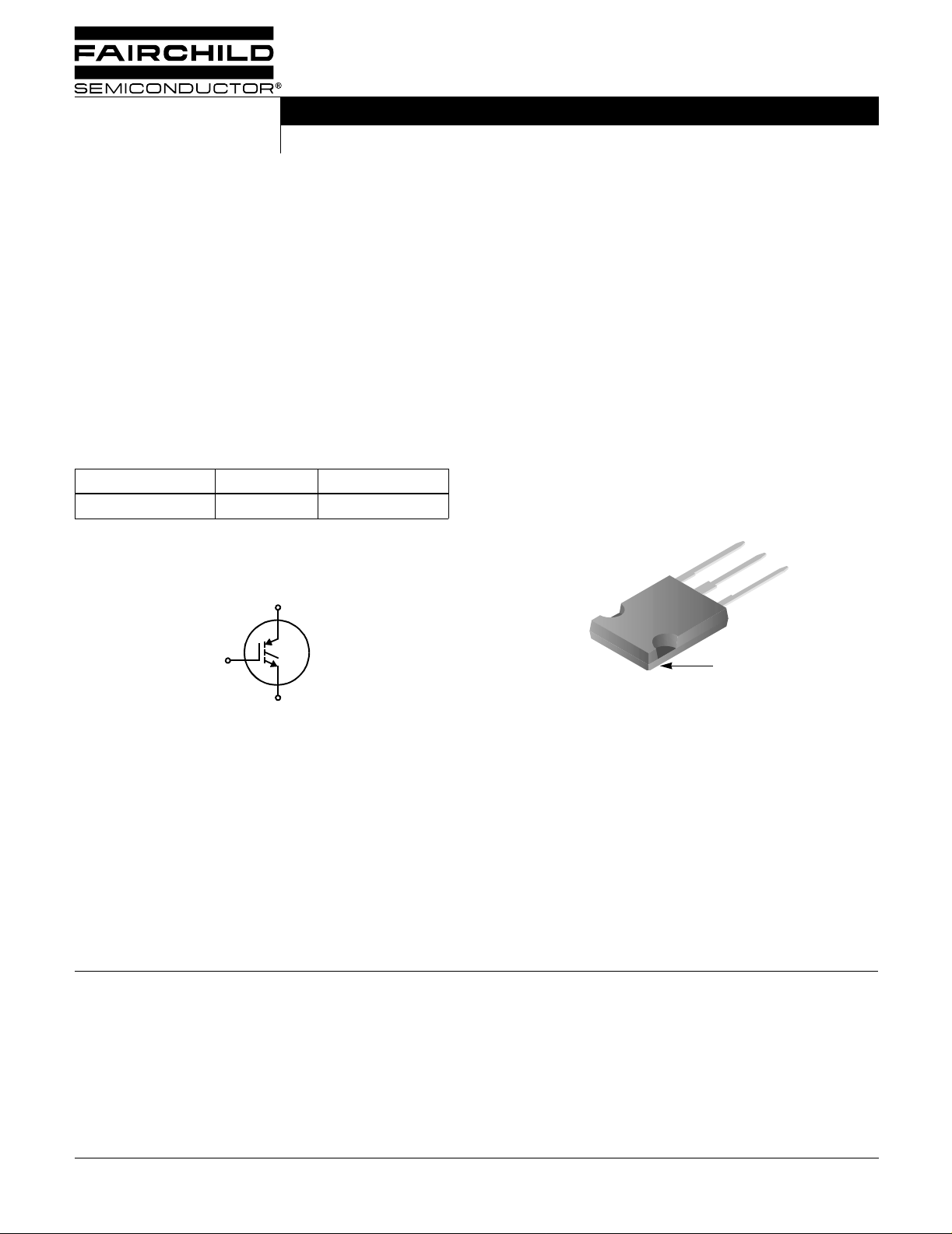
Symbol
C
File Number 4829
Features
• >100kHz Operation at 390V, 30A
• 200kHz Operation at 390V, 18A
• 600V Switching SOA Capability
• Typical Fall Time. . . . . . . . . . . . . . . . . 60ns at T
• Low Conduction Loss
Packaging
JEDEC STYLE TO-247
E
C
G
= 125oC
J
G
E
FAIRCHILD CORPORATION IGBT PRODUCT IS COVERED BY ONE OR MORE OF THE FOLLOWING U.S. PATENTS
4,364,073 4,417,385 4,430,792 4,443,931 4,466,176 4,516,143 4,532,534 4,587,713
4,598,461 4,605,948 4,620,211 4,631,564 4,639,754 4,639,762 4,641,162 4,644,637
4,682,195 4,684,413 4,694,313 4,717,679 4,743,952 4,783,690 4,794,432 4,801,986
4,803,533 4,809,045 4,809,047 4,810,665 4,823,176 4,837,606 4,860,080 4,883,767
4,888,627 4,890,143 4,901,127 4,904,609 4,933,740 4,963,951 4,969,027
COLLECTOR
(BACK METAL)
©2003 Fairchild Semiconductor Corporation HGTG30N60A4 Rev. B1
HGTG30N60A4
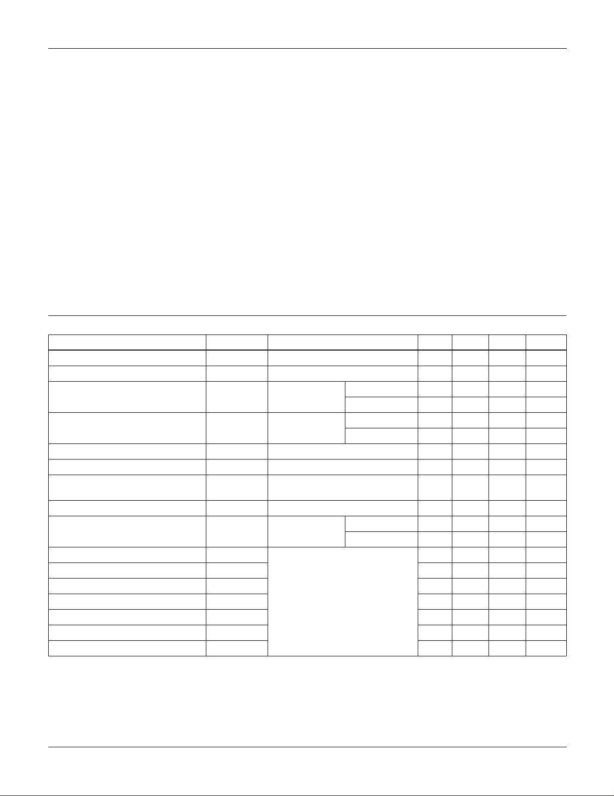
Absolute Maximum Ratings T
= 25oC, Unless Otherwise Specified
C
HGTG30N60A4 UNITS
Collector to Emitter Voltage . . . . . . . . . . . . . . . . . . . . . . . . . . BV
CES
600 V
Collector Current Continuous
At T
= 25oC . . . . . . . . . . . . . . . . . . . . . . . . . . . . . . . . . . . . . I
C
= 110oC . . . . . . . . . . . . . . . . . . . . . . . . . . . . . . . . . . . I
At T
C
Collector Cu rrent Pulsed (No te 1) . . . . . . . . . . . . . . . . . . . . . . . .I
Gate to Emitter Voltage Continuous. . . . . . . . . . . . . . . . . . . . . V
Gate to Emitter Voltage Pulsed . . . . . . . . . . . . . . . . . . . . . . . .V
Switching Safe Operating Area at T
Powe r Dissipation Total at T
C
Power Dissipation Derating T
= 150oC, Figure 2 . . . . .SSOA 150A at 600V
J
= 25oC . . . . . . . . . . . . . . . . . . . . . P
> 25oC . . . . . . . . . . . . . . . . . . . . . . . 3.7 W/oC
C
Operating and Storage Junction Temperature Range . . . . .T
C25
C110
CM
GES
GEM
D
, T
J
STG
Maximum Lead T emperature for Soldering
Leads at 0.063in (1.6mm) from Case for 10s. . . . . . . . . . . . . . . T
Package Body for 10s, See Techbrief 334 . . . . . . . . . . . . . . T
CAUTION: Stresses above those listed in “A bsolute Maximu m Rating s” may cause per manent d amage to t he device. This is a str ess on ly rating and operation o f the
device at these or any other conditions above those indicated in the operational sections of this specification is not implied.
L
PKG
75 A
60 A
240 A
±20 V
±30 V
463 W
-55 to 150
300
260
o
C
o
C
o
C
NOTE:
1. Pulse width limited by maximum junction temperature.
Electrical Specifications T
= 25oC, Unless Otherwise Specified
J
PARAMETER SYMBOL TEST CONDITIONS MIN TYP MAX UNITS
Collector to Emitter Breakdown Voltage BV
Emitter to Collector Breakdown Voltage BV
Collector to Emitter Leakage Current I
Collector to Emitter Saturation Voltage V
Gate to Emitter Threshold Voltage V
Gate to Emitter Leakage Current I
CES
ECS
CES
CE(SAT)IC
GE(TH)
GES
Switching SOA SSOA T
Gate to Emitter Plateau Voltage V
On-State Gate Charge Q
Current Turn-On Delay Time t
Current Rise Time t
Current Turn-Off Delay Time t
Current Fall Time t
Turn-On Energy (Note 2) E
Turn-On Energy (Note 2) E
Turn-Off Energy (Note 3) E
GEP
g(ON)
d(ON)I
rI
d(OFF)I
fI
ON1
ON2
OFF
IC = 250µA, VGE = 0V 600 - - V
IC = -10mA, V
= 0V 20 - - V
GE
VCE = 600V TJ = 25oC - - 250 µA
T
= 125oC--4.0mA
J
= 30A,
V
GE
= 15V
T
= 25oC-1.82.6V
J
T
= 125oC-1.62.0V
J
IC = 250µA, VCE = 600V 4.5 5.2 7.0 V
VGE = ±20V - - ±250 nA
= 150oC, RG = 3Ω, VGE = 15V
J
L = 100µH, V
CE
= 600V
150 - - A
IC = 30A, VCE = 300V - 8.5 - V
IC = 30A,
= 300V
V
CE
IGBT and Diode at TJ = 25oC
I
= 30A
CE
= 390V
V
CE
=15V
V
GE
R
= 3Ω
G
L = 200µH
Test Circuit - (Figure 20)
V
= 15V - 225 270 nC
GE
V
= 20V - 300 360 nC
GE
-25- ns
-12- ns
- 150 - ns
-38- ns
- 280 - µJ
- 600 - µJ
- 240 350 µJ
©2003 Fairchild Semiconductor Corporation HGTG30N60A4 Rev. B1
HGTG30N60A4
Electrical Specifications T
= 25oC, Unless Otherwise Specified (Continued)
J
PARAMETER SYMBOL TEST CONDITIONS MIN TYP MAX UNITS
Current Turn-On Delay Time t
d(ON)I
Current Rise Time t
Current Turn-Off Delay Time t
d(OFF)I
Current Fall Time t
Turn-On Energy (Note 2) E
Turn-On Energy (Note 2) E
Turn-Off Energy (Note 3) E
Thermal Resistance Junction To Case R
rI
fI
ON1
ON2
OFF
θJC
IGBT and Diode at TJ = 125oC
I
= 30A
CE
= 390V
V
CE
= 15V
V
GE
R
= 3Ω
G
L = 200µH
Test Circuit - (Figure 20)
NOTES:
2. Values for two Turn-On loss conditions are shown for the convenience of the circuit designer. E
is the turn-on loss when a typical diode is used in the test circuit and the diode is at the same T
Figure 20.
3. Turn-Off Energy Loss (E
at the point where the collector current equals zero (I
) is defined as the integral of the instantaneous power loss starting at the trailing edge of the input pulse and ending
OFF
= 0A). All devices were tested per JEDEC Standard No. 24-1 Method for Measurement
CE
of Power Device Turn-Off Switching Loss. This test method produces the true total Turn-Off Energy Loss.
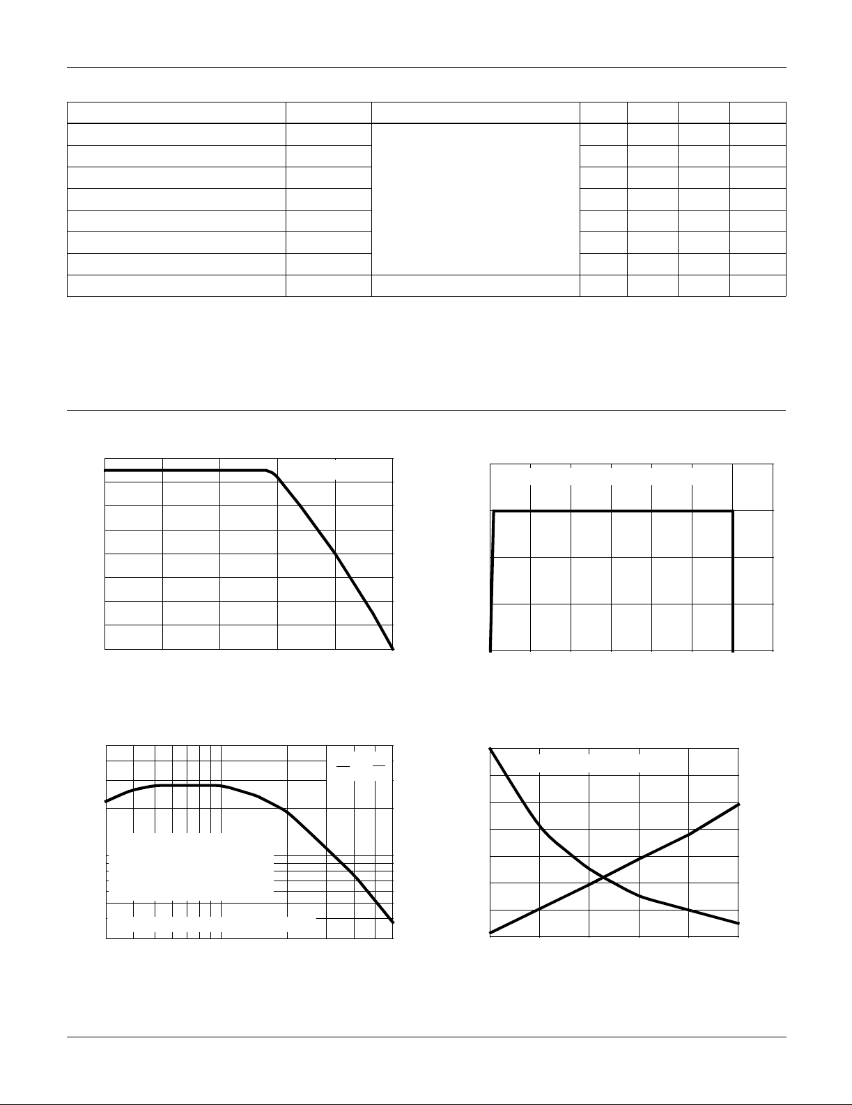
Typical Performance Curves Unless Otherwise Specified
60
70
60
50
40
30
V
= 15V
GE
200
TJ = 150oC, RG = 3Ω, V
150
100
-24- ns
-11- ns
- 180 200 ns
-5870ns
- 280 - µJ
- 1000 1160 µJ
- 450 750 µJ
- - 0.27
is the turn-on loss of the IGBT only. E
ON1
as the IGBT. The diode type is specified in
J
= 15V, L = 500µH
GE
o
C/W
ON2
20
, DC COLLECTOR CURRENT (A)
10
CE
I
0
25 75 100 125 150
50
TC, CASE TEMPERATURE (oC)
FIGURE 1. DC COLLECTOR CURRENT vs CASE
TEMPERATURE
500
300
f
= 0.05 / (t
MAX1
f
= (PD - PC) / (E
MAX2
100
PC = CONDUCTION DISSIPATION
(DUTY FACTOR = 50%)
R
= 0.27oC/W, SEE NOTES
ØJC
, OPERATING FREQUENCY (kHz)
MAX
TJ = 125oC, RG = 3Ω, L = 200µH, V
f
30
3
d(OFF)I
ICE, COLLECTOR TO EMITTER CURRENT (A)
+ t
ON2
d(ON)I
+ E
OFF
)
)
= 390V
CE
75
V
T
C
o
C
FIGURE 3. OPERA TING FREQUENCY vs COLLECTOR T O
EMITTER CURRENT
GE
15V
50
, COLLECTOR TO EMITTER CURRENT (A)
0
CE
I
VCE, COLLECTOR TO EMITTER VOLTAGE (V)
300 400200100 500 600
7000
FIGURE 2. MINIMUM SWITCHING SAFE OPERATING AREA
18
16
14
12
10
8
6
, SHORT CIRCUIT WITHSTAND TIME (µs)
4
SC
t
6010 30
10 11 12 15
VCE = 390V, RG = 3Ω, TJ = 125oC
13 14
V
, GATE TO EMITTER V OLTAGE (V)
GE
I
SC
t
SC
900
800
700
600
500
400
300
200
, PEAK SHORT CIRCUIT CURRENT (A)
SC
I
FIGURE 4. SHORT CIRCUIT WITHSTAND TIME
©2003 Fairchild Semiconductor Corporation HGTG30N60A4 Rev. B1
 Loading...