

Fairchild Semiconductor HGTG27N120BN Datasheet
HGTG27N120BN / HGT5A27N120BN
Data Sheet August 2002
72A, 1200V, NPT Series N-Channel IGBT
The HGTG27N120BN and HGT5A27N120BN are Non-
Punch Through (NPT) IGBT design. This is a new member
of the MOS gated high vol tage s w itch ing IGBT fa mily. IGBTs
combine the best features of MOSFETs and bipolar
transistors. This device has the high input impedance of a
MOSFET and the low on-state conduction loss of a bipolar
transistor.
The IGBT is ideal for many high voltage switching
applications operating at moderate frequencies where low
conduction losses are essential, such as: AC and DC motor
controls, pow er su ppl ies and drivers for solenoids, relays
and contactors.
Formerly Developmental Type TA49280.
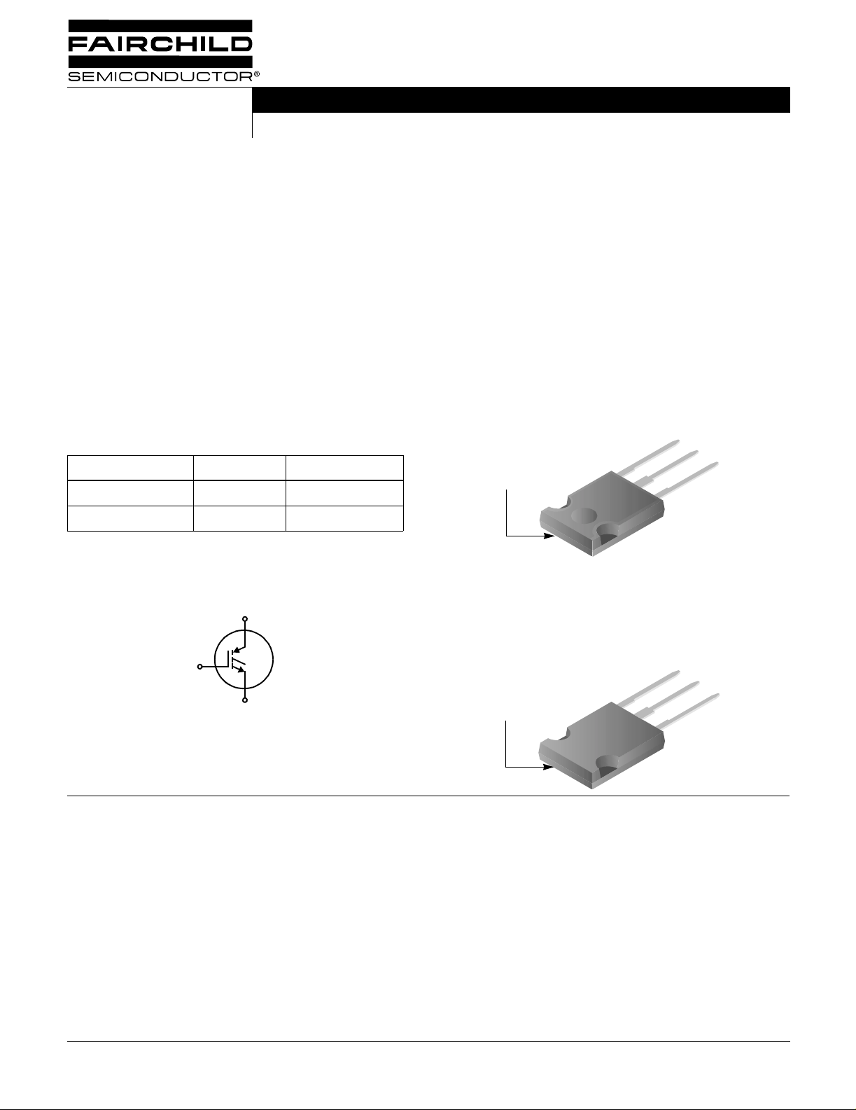
Ordering Information
PART NUMBER PACKAGE BRAND
HGTG27N120BN TO-247 27N120BN
HGT5A27N120BN TO-247-ST 27N120BN
NOTE: When ordering, use the entire part number.
Features
• 72A, 1200V, TC = 25oC
• 1200V Switching SOA Capability
• Typical Fall Time. . . . . . . . . . . . . . . . 140ns at T
• Short Circuit Rating
• Low Conduction Loss
• Thermal Impedance SPICE Model
Temperature Compensating SABER™ Model
www.fairchildsemi.com
• Avalanche Rated
Packaging
JEDEC STYLE TO-247
E
COLLECTOR
(BOTTOM SIDE
METAL)
C
G
= 150oC
J
Symbol
C
JEDEC STYLE TO-247-ST
G
COLLECTOR
(BOTTOM SIDE
E
FAIRCHILD SEMICONDUCTOR IGBT PRODUCT IS COVERED BY ONE OR MORE OF THE FOLLOWING U.S. PATENTS
4,364,073 4,417,385 4,430,792 4,443,931 4,466,176 4,516,143 4,532,534 4,587,713
4,598,461 4,605,948 4,620,211 4,631,564 4,639,754 4,639,762 4,641,162 4,644,637
4,682,195 4,684,413 4,694,313 4,717,679 4,743,952 4,783,690 4,794,432 4,801,986
4,803,533 4,809,045 4,809,047 4,810,665 4,823,176 4,837,606 4,860,080 4,883,767
4,888,627 4,890,143 4,901,127 4,904,609 4,933,740 4,963,951 4,969,027
METAL)
E
C
G
©2002 Fairchild Semiconductor Corporation HGTG27N120BN / HGT5A27N12BN Rev. C1
HGTG27N120BN / HGT5A27N120BN
Absolute Maximum Ratings T
= 25oC, Unless Otherwise Specified
C
HGTG27N120BN UNITS
Collector to Emitter Voltage . . . . . . . . . . . . . . . . . . . . . . . . . . . . . . . . . . . . . . . . . . . . . .BV
CES
1200 V
Collector Current Continuous
= 25oC . . . . . . . . . . . . . . . . . . . . . . . . . . . . . . . . . . . . . . . . . . . . . . . . . . . . . . . . . I
At T
C
At T
= 110oC . . . . . . . . . . . . . . . . . . . . . . . . . . . . . . . . . . . . . . . . . . . . . . . . . . . . . . . I
C
Collector Current Pulsed (Note 1) . . . . . . . . . . . . . . . . . . . . . . . . . . . . . . . . . . . . . . . . . . . I
Gate to Emitter Voltage Continuous. . . . . . . . . . . . . . . . . . . . . . . . . . . . . . . . . . . . . . . . .V
Gate to Emitter Voltage Pulsed . . . . . . . . . . . . . . . . . . . . . . . . . . . . . . . . . . . . . . . . . . . .V
Switching Safe Operating Area at T
Powe r Dissipation Total at T
C
Power Dissipation Derating T
= 150oC (Figure 2) . . . . . . . . . . . . . . . . . . . . . . . SSOA 150A at 1200V
J
= 25oC . . . . . . . . . . . . . . . . . . . . . . . . . . . . . . . . . . . . . . . . . P
> 25oC . . . . . . . . . . . . . . . . . . . . . . . . . . . . . . . . . . . . . . . . . . 4.0 W/oC
C
Forward Voltage Avalanche Energy (Note 2). . . . . . . . . . . . . . . . . . . . . . . . . . . . . . . . . . . E
Operating and Storage Junction Temperature Range . . . . . . . . . . . . . . . . . . . . . . . . T
Maximum Lead T emperature for Soldering . . . . . . . . . . . . . . . . . . . . . . . . . . . . . . . . . . . . . T
Short Circuit Withstand Time (Note 3) at V
Short Circuit Withstand Time (Note 3) at V
CAUTION: Stresses above those listed in “A bsolute Maximu m Rating s” may cause per manent d amage to t he device. This is a str ess on ly rating and operation o f the
device at these or any other conditions above those indicated in the operational sections of this specification is not implied.
= 15V. . . . . . . . . . . . . . . . . . . . . . . . . . . . . .t
GE
= 12V. . . . . . . . . . . . . . . . . . . . . . . . . . . . . .t
GE
C25
C110
CM
GES
GEM
D
AV
, T
J
STG
L
SC
SC
72 A
34 A
216 A
±20 V
±30 V
500 W
135 mJ
-55 to 150
260
8 µs
15 µs
o
C
o
C
NOTES:
1. Pulse width limited by Max junction temperature.
= 30A, L = 400µH, TJ = 125oC
2. I
CE
3. V
= 960V, TJ = 125oC, RG = 3Ω.
CE(PK)
Electrical Specifications T
= 25oC, Unless Otherwise Specified
C
PARAMETER SYMBOL TEST CONDITIONS MIN TYP MAX UNITS
Collector to Emitter Breakdown Voltage BV
Emitter to Collector Breakdown Voltage BV
Collector to Emitter Leakage Current I
Collector to Emitter Saturation Voltage V
Gate to Emitter Threshold Voltage V
Gate to Emitter Leakage Current I
CES
ECS
CES
CE(SAT)IC
GE(TH)
GES
Switching SOA SSOA T
Gate to Emitter Plateau Voltage V
On-State Gate Charge Q
Current Turn-On Delay Time t
Current Rise Time t
Current Turn-Off Delay Time t
Current Fall Time t
Turn-On Energy (Note 5) E
Turn-On Energy (Note 5) E
Turn-Off Energy (Note 4) E
GEP
G(ON)
d(ON)I
rI
d(OFF)I
fI
ON1
ON2
OFF
IC = 250µA, VGE = 0V 1200 - - V
IC = 10mA, V
= 0V 15 - - V
GE
VCE = 1200V TC = 25oC - - 250 µA
= 125oC - 300 - µA
T
C
T
= 150oC--4mA
C
= 27A,
= 15V
V
GE
IC = 250µA, VCE = V
T
= 25oC - 2.45 2.7 V
C
= 150oC-3.84.2V
T
C
GE
66.6 - V
VGE = ±20V - - ±250 nA
= 150oC, RG = 3Ω, VGE = 15V,
J
L = 200µH, V
IC = I
, VCE = 0.5 BV
C110
IC = 27A,
V
= 600V
CE
CE(PK)
= 1200V
CES
= 15V - 270 325 nC
V
GE
V
= 20V - 350 420 nC
GE
IGBT and Diode at TJ = 25oC,
= 27A,
I
CE
= 960V,
V
CE
V
= 15V,
GE
= 3Ω,
R
G
L = 1mH,
Test Circuit (Figure 18)
150 - - A
-9.2- V
-2430ns
-2025ns
- 195 240 ns
- 80 120 ns
-2.2- mJ
-2.73.3mJ
-2.32.8mJ
©2002 Fairchild Semiconductor Corporation HGTG27N120BN / HGT5A27N12BN Rev. C1
HGTG27N120BN / HGT5A27N120BN
Electrical Specifications T
= 25oC, Unless Otherwise Specified (Continued)
C
PARAMETER SYMBOL TEST CONDITIONS MIN TYP MAX UNITS
Current Turn-On Delay Time t
d(ON)I
Current Rise Time t
Current Turn-Off Delay Time t
d(OFF)I
Current Fall Time t
Turn-On Energy (Note 5) E
Turn-On Energy (Note 5) E
Turn-Off Energy (Note 4) E
Thermal Resistance Junction To Case R
rI
fI
ON1
ON2
OFF
θJC
IGBT and Diode at TJ = 150oC,
= 27A,
I
CE
= 960V,
V
CE
V
= 15V,
GE
= 3Ω,
R
G
L = 1mH,
Test Circuit (Figure 18)
NOTES:
4. Turn-Off Energy Loss (E
at the point where the collector current equals zero (I
of Power Device Turn-Off Switching Loss. This test method produces the true total Turn-Off Energy Loss.
) is defined as the integral of the instantaneous power loss starting at the trailing edge of the input pulse and ending
OFF
= 0A). All devices were tested per JEDEC Standard No. 24-1 Method for Measurement
CE
5. Values for two Turn-On loss conditions are shown for the convenience of the circuit designer. E
is the turn-on loss when a typical diode is used in the test circuit and the diode is at the same T
Figure 18.
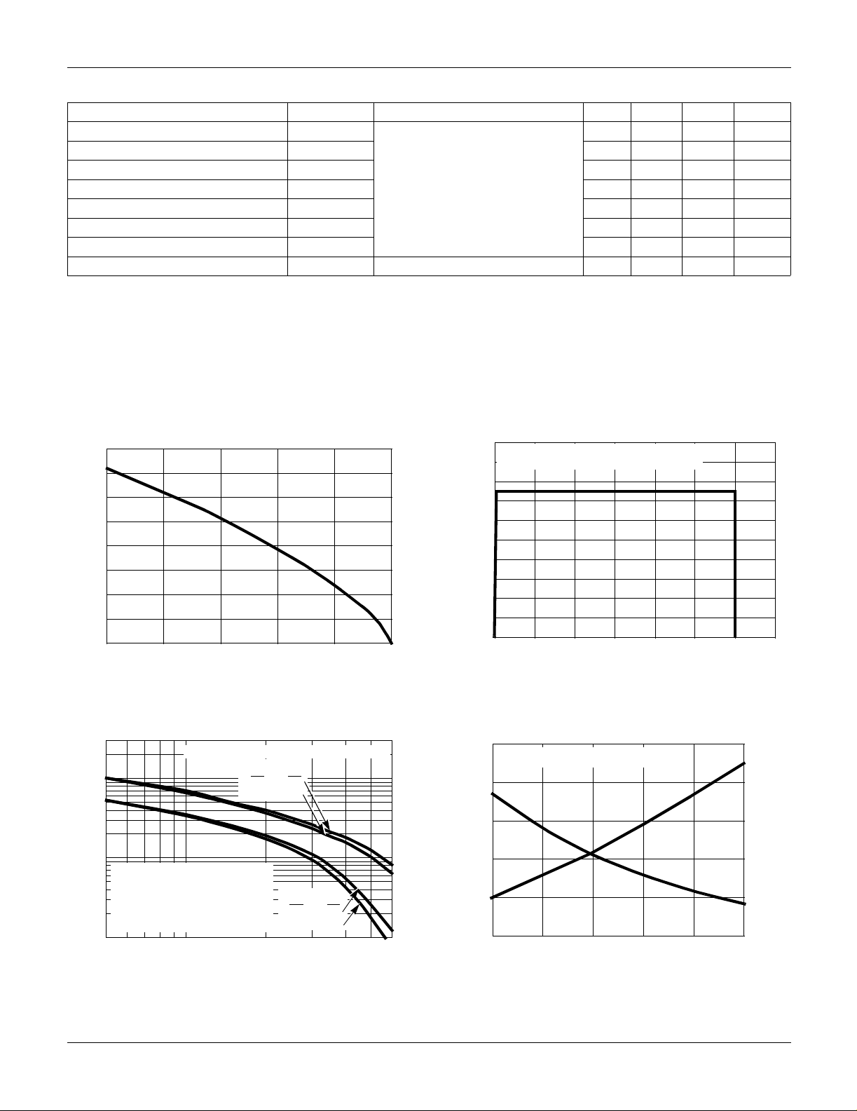
Typical Performance Curves Unless Otherwise Specified
80
70
60
50
= 15V
V
GE
200
TJ = 150oC, RG = 3Ω, V
160
120
-2228ns
-2025ns
- 220 280 ns
- 140 200 ns
-2.7- mJ
-5.16.5mJ
-3.44.2mJ
- - 0.25
is the turn-on loss of the IGBT only. E
ON1
as the IGBT. The diode type is specified in
J
= 15V, L = 200µH
GE
o
C/W
ON2
40
30
20
, DC COLLECTOR CURRENT (A)
10
CE
I
0
25 75 100 125 150
50
TC, CASE TEMPERATURE (oC)
FIGURE 1. DC COLLECTOR CURRENT vs CASE
TEMPERATURE
, OPERATING FREQUENCY (kHz)
MAX
f
100
50
10
f
= 0.05 / (t
MAX1
= (PD - PC) / (E
f
MAX2
= CONDUCTION DISSIPATION
P
C
(DUTY FACTOR = 50%)
R
= 0.25oC/W, SEE NOTES
ØJC
1
5
, COLLECTOR TO EMITTER CURRENT (A)
I
CE
TJ = 150oC, RG = 3Ω, L = 1mH, V
T
V
C
GE
o
15V
75
C
o
12V
C
75
+ t
d(OFF)I
ON2
10
d(ON)I
+ E
OFF
)
)
T
C
110
110oC
CE
V
GE
o
15V
C
12V
= 960V
80
40
, COLLECTOR TO EMITTER CURRENT (A)
0
CE
I
0
V
, COLLECTOR TO EMITTER VOLTAGE (V)
CE
600 800400200 1000 1200
1400
FIGURE 2. MINIMUM SWITCHING SAFE OPERATING AREA
50
VCE = 960V, RG = 3Ω, TJ = 125oC
40
30
20
10
, SHORT CIRCUIT WITHSTAND TIME (µs)
SC
0
t
6020
11 12 13 14 15 16
VGE, GATE TO EMITTER VOLTAGE (V)
500
I
SC
400
300
200
t
SC
100
, PEAK SHORT CIRCUIT CURRENT (A)
SC
I
0
FIGURE 3. OPERATING FREQUENCY vs COLLECT OR TO
FIGURE 4. SHORT CIRCUIT WITHSTAND TIME
EMITTER CURRENT
©2002 Fairchild Semiconductor Corporation HGTG27N120BN / HGT5A27N12BN Rev. C1
 Loading...