

Fairchild Semiconductor HGTG20N60C3D Datasheet
Data Sheet December 2001
HGTG20N60C3D
45A, 600V, UFS Series N-Channel IGBT
with Anti-Parallel Hyperfast Diode
The HGTG20N60C3D is a MOS gated high voltage
switching device combining the best feat ures of MOSFETs
and bipolar transistors. This device has the high input
impedance of a MOSFET and the low on-state conduction
loss of a bipolar transistor. The much lower on-state voltage
drop varies only moderately between 25
o
C and 150oC. The
IGBT used is dev e lopme nt type TA49178 . The diode used i n
anti-parallel with the IGBT is the RHRP3060 (TA49063).
The IGBT is ideal for many high voltage sw itc hi ng
applications operating at moderate frequencies where low
conduction losses are ess ential, such as: AC and DC motor
controls, power supplies and drivers for solenoids, relays
and contactors.
Formerly developmental type TA49179.
Ordering Information
PART NUMBER PACKAGE BRAND
HGTG20N60C3D TO-247 G20N60C3D
NOTE: When ordering, use the entire part number.
Features
• 45A, 600V, TC = 25oC
• 600V Switching SOA Capability
• Typical Fall Time. . . . . . . . . . . . . . . . 108ns at T
• Short Circuit Rating
• Low Conduction Loss
• Hyperfast Anti-Parallel Diode
Packaging
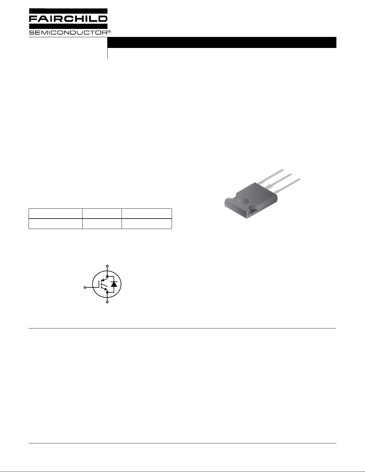
JEDEC STYLE TO-247
E
C
G
= 150oC
J
Symbol
C
G
E
FAIRCHILD SEMICONDUCTOR IGBT PRODUCT IS COVERED BY ONE OR MORE OF THE FOLLOWING U.S. PATENTS
4,364,073 4,417,385 4,430,792 4,443,931 4,466,176 4,516,143 4,532,534 4,587,713
4,598,461 4,605,948 4,620,211 4,631,564 4,639,754 4,639,762 4,641,162 4,644,637
4,682,195 4,684,413 4,694,313 4,717,679 4,743,952 4,783,690 4,794,432 4,801,986
4,803,533 4,809,045 4,809,047 4,810,665 4,823,176 4,837,606 4,860,080 4,883,767
4,888,627 4,890,143 4,901,127 4,904,609 4,933,740 4,963,951 4,969,027
©2001 Fairchild Semiconductor Corpo ration HGTG20N60C3D Rev. B
HGTG20N60C3D
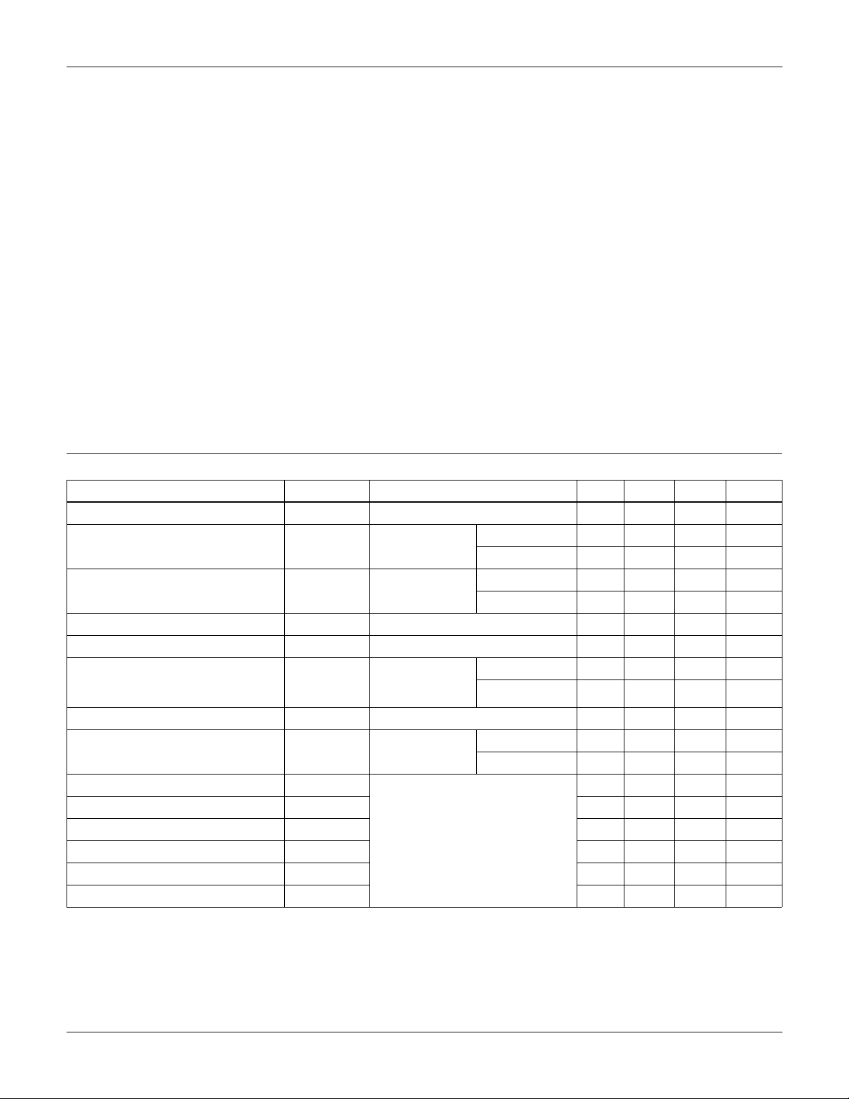
Absolute Maximum Ratings
TC = 25oC, Unless Otherwise Specified
HGTG20N60C3D UNITS
Collector to Emitter Voltage . . . . . . . . . . . . . . . . . . . . . . . . . . . . . . . . . . . . . . . . . . . . . . BV
CES
600 V
Collector Current Continuous
= 25oC . . . . . . . . . . . . . . . . . . . . . . . . . . . . . . . . . . . . . . . . . . . . . . . . . . . . . . . . . I
At T
C
= 110oC . . . . . . . . . . . . . . . . . . . . . . . . . . . . . . . . . . . . . . . . . . . . . . . . . . . . . . . I
At T
C
Collector Current Pulsed (Note 1) . . . . . . . . . . . . . . . . . . . . . . . . . . . . . . . . . . . . . . . . . . . I
Gate to Emitter Voltage Continuous. . . . . . . . . . . . . . . . . . . . . . . . . . . . . . . . . . . . . . . . . V
Gate to Emitter Voltage Pulsed . . . . . . . . . . . . . . . . . . . . . . . . . . . . . . . . . . . . . . . . . . . . V
Switching Safe Operating Area at T
Pow er Dissi pation Total at T
C
Power Dissipation Derating T
= 150oC (Figure 2) . . . . . . . . . . . . . . . . . . . . . . . SSOA 20A at 600V
J
= 25oC . . . . . . . . . . . . . . . . . . . . . . . . . . . . . . . . . . . . . . . . . P
> 25oC . . . . . . . . . . . . . . . . . . . . . . . . . . . . . . . . . . . . . . . . . . 1.32 W/oC
C
Operating and Storage Junction Temperature Range . . . . . . . . . . . . . . . . . . . . . . . . T
Maximum Lead Temperature for Soldering . . . . . . . . . . . . . . . . . . . . . . . . . . . . . . . . . . . . . T
Short Circuit Withstand Time (Not e 2) at V
Short Circuit Withstand Time (Not e 2) at V
CAUTION: Stresses above those listed in “A bsolute Maximu m Rating s” may cause per manent d amage to t he device. This is a str ess on ly rating and operation o f the
device at these or any other conditions above those indicated in the operational sections of this specification is not implied.
= 12V. . . . . . . . . . . . . . . . . . . . . . . . . . . . . .t
GE
= 10V. . . . . . . . . . . . . . . . . . . . . . . . . . . . . .t
GE
C25
C110
CM
GES
GEM
D
, T
J
STG
L
SC
SC
45 A
20 A
300 A
±20 V
±30 V
164 W
-55 to 150
260
4 µs
10 µs
o
C
o
C
NOTES:
1. Pulse width limited by maximum junction temperature.
2. V
Electrical Specifications
= 360V, TJ = 125oC, RG = 10Ω.
CE(PK)
TC = 25oC, Unless Otherwise Specified
PARAMETER SYMBOL TEST CONDITIONS MIN TYP MAX UNITS
Collector to Emitter Breakdown Voltage BV
Collector to Emitter Leakage Current I
Collector to Emitter Saturation Voltage V
Gate to Emitter Threshold Voltage V
Gate to Emitter Leakage Current I
CES
CES
CE(SAT)IC
GE(TH)
GES
Switching SOA SSOA T
Gate to Emitter Plateau Voltage V
On-State Gate Charge Q
Current Turn-On Delay Time t
Current Rise Time t
Current Turn-Off Delay Time t
Current Fall Time t
Turn-On Energy E
Turn-Off Energy (Note 3) E
GEP
G(ON)
d(ON)I
rI
d(OFF)I
fI
ON
OFF
IC = 250µA, VGE = 0V 600 - - V
VCE = BV
V
= I
GE
C110
= 15V
CES
IC = 250µA, VCE = V
TC = 25oC - - 250 µA
T
= 150oC--5.0mA
C
T
= 25oC-1.41.8V
C
= 150oC-1.51.9V
T
C
GE
3.4 4.8 6.3 V
VGE = ±20V - - ±250 nA
= 150oC, RG =
J
GE
= 15V,
10Ω, V
L = 100µH
ICE = I
ICE = I
, VCE = 0.5 BV
C110
C110
VCE = 0.5 BV
IGBT and Diode at TJ = 25oC
= I
I
CE
C110
VCE = 0.8 BV
VGE = 15V
R
= 10Ω
G
L = 1mH
Test Circuit (Figure 19)
V
= 480V 120 - - A
CE
= 600V 20 - - A
V
CE
CES
-8.4- V
VGE = 15V - 91 110 nC
CES
V
= 20V - 122 145 nC
GE
-2832ns
CES
-2428ns
- 151 210 ns
-5598ns
- 500 550 µJ
- 500 700 µJ
©2001 Fairchild Semiconductor Corpo ration HGTG20N60C3D Rev. B
0
0
HGTG20N60C3D
Electrical Specifications
TC = 25oC, Unless Otherwise Specified (Continued)
PARAMETER SYMBOL TEST CONDITIONS MIN TYP MAX UNITS
Current Turn-On Delay Time t
d(ON)I
Current Rise Time t
Current Turn-Off Delay Time t
d(OFF)I
Current Fall Time t
Turn-On Energy E
Turn-Off Energy (Note 3) E
Diode Forward Voltage V
Diode Reverse Recovery Time t
Thermal Resistance Junction To Case R
rI
fI
ON
OFF
EC
rr
θJC
IGBT and Diode at TJ = 150oC
= I
I
CE
C110
VCE = 0.8 BV
CES
VGE = 15V
= 10Ω
R
G
L = 1mH
Test Circuit (Figure 19)
IEC = 20A - 1.5 1.9 V
IEC = 20A, dIEC/dt = 200A/µs--55ns
= 2A, dIEC/dt = 200A/µs - 32 47 ns
I
EC
IGBT - - 0.76
Diode - - 1.2
NOTES:
3. Turn-Off Energy Loss (E
at the point where the collector current equals zero (I
of Power Device Turn-Off Switching Loss. This test method produces the true total Turn-Off Energy Loss.
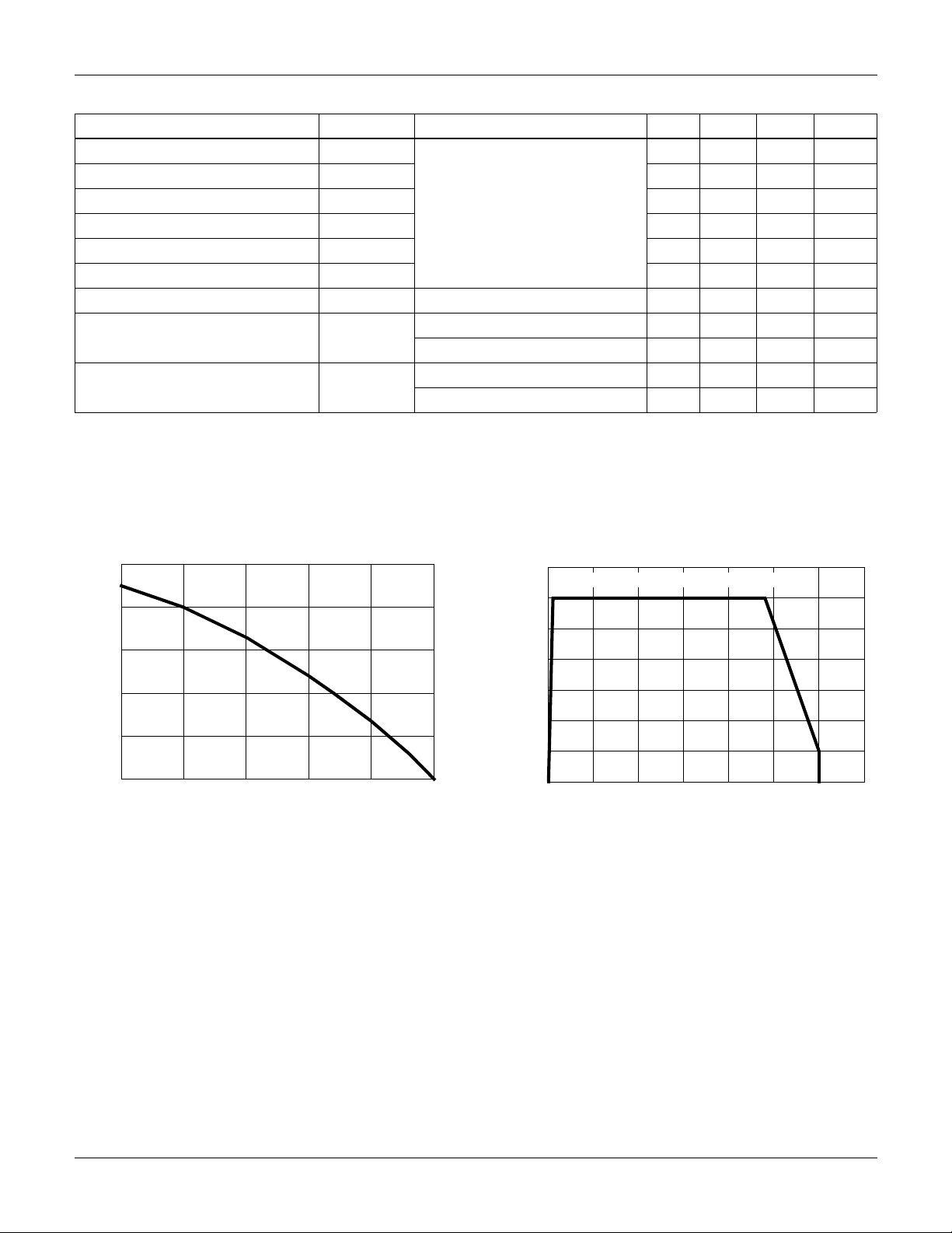
Typical Performance Curves
) is defined as the integral of the instantaneous power loss starting at the trailing edge of the input pulse and ending
OFF
= 0A). All devices were tested per JEDEC Standard No. 24-1 Method for Measurement
CE
Unless Otherwise Specified
-2832ns
-2428ns
- 280 450 ns
- 108 210 ns
-1.01.1mJ
-1.21.7mJ
o
C/W
o
C/W
50
40
30
20
10
, DC COLLECTOR CURRENT (A)
CE
I
0
25 75 100 125 15
50
TC, CASE TEMPERATURE (oC)
FIGURE 1. DC COLLECTOR CURRENT vs CASE
TEMPERATURE
= 15V
V
GE
140
TJ = 150oC, RG = 10Ω, V
120
100
80
60
40
20
, COLLECTOR TO EMITTER CURRENT (A)
0
CE
I
0
VCE, COLLECTOR TO EMITTER VOLTAGE (V)
= 15V, L = 100µH
GE
300 400200100 500 600
70
FIGURE 2. MINIMUM SWITCHING SAFE OPERATING AREA
©2001 Fairchild Semiconductor Corpo ration HGTG20N60C3D Rev. B
 Loading...