

Fairchild Semiconductor HGTG20N60A4D Datasheet
HGTG20N60A4D, HGT4E20N60A4DS
Data Sheet APRIL 2002
600V, SMPS Series N-Channel IGBT with
Anti-Parallel Hyperfast Diode
This family of MOS gat ed high voltage switching devices
combine the best f eatures of MOSFETs and bipolar
transist ors. These devices hav e the high input i m pedance of
a MOSFET and the low on-st ate conduction l oss of a bipolar
transist or. The much lower on-state voltage drop v ari es only
moderately bet ween 25
o
C and 150oC. Th e IGBT used is the
dev elopment type TA49339. The diode used in anti-parallel
is the development type TA49372.
These IGBT’s are ideal for many high volt age switching
applications operating at high frequencies where low
conduction losses are essential. These devices have been
optimized for high frequency switch mode power
supplies.
Formerly Developmental Type TA49341.
Ordering Information
PART NUMBER PACKAGE BRAND
HGTG20N60A4D TO-247 20N60A4D
HGT4E20N60A4DS TO-268 20N60A4DS
NOTE: When ordering, use the entire part number.
Features
• >100kHz Opera ti on At 390V, 20A
• 200kHz Operation At 390V, 12A
• 600V Switching SO A Capability
• Typical Fall Ti m e . . . . . . . . . . . . . . . . .55ns at T
• Low Conduction Loss
• Temperature Compensating SABER™ Model
www.fairchildsemi.com
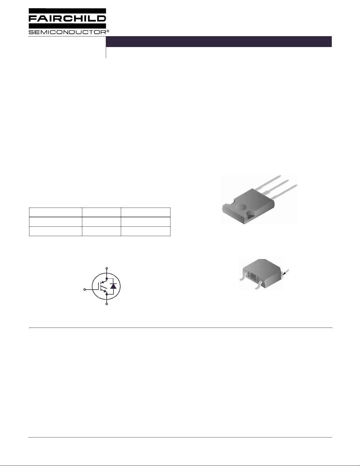
Packaging
JEDEC STYLE TO-247
E
C
G
TO-268AA
= 125oC
J
Symbol
C
C
G
G
E
FAIRCHILD SEMICONDUCTOR IGBT PRODUCT IS COVERED BY ONE OR MORE OF THE FOLLOWING U.S. PATENTS
4,364,073 4,417,385 4,430,792 4,443,931 4,466,176 4,516,143 4,532,534 4,587,713
4,598,461 4,605,948 4,620,211 4,631,564 4,639,754 4,639,762 4,641,162 4,644,637
4,682,195 4,684,413 4,694,313 4,717,679 4,743,952 4,783,690 4,794,432 4,801,986
4,803,533 4,809,045 4,809,047 4,810,665 4,823,176 4,837,606 4,860,080 4,883,767
4,888,627 4,890,143 4,901,127 4,904,609 4,933,740 4,963,951 4,969,027
E
©2002 Fairchild Semiconductor Corporation HGTG20N60A4D, HGT4E20N60A4DS Rev. C
HGTG20N60A4D, HGT4E20N60A4DS
Absolute Maximum Ratings T
= 25oC, Unless Otherwise Specified
C
HGTG20N60A4D,
HGT4E20N60A4DS UNITS
Collector to Emitter Voltage . . . . . . . . . . . . . . . . . . . . . . . . . . . . . . . . . . . . . . . . . . . . . .BV
CES
600 V
Collector Current Continuous
At T
= 25oC . . . . . . . . . . . . . . . . . . . . . . . . . . . . . . . . . . . . . . . . . . . . . . . . . . . . . . . . .I
C
At T
= 110oC . . . . . . . . . . . . . . . . . . . . . . . . . . . . . . . . . . . . . . . . . . . . . . . . . . . . . . . I
C
Collector Current Pulsed (Note 1) . . . . . . . . . . . . . . . . . . . . . . . . . . . . . . . . . . . . . . . . . . . I
Gate to Emitter Voltage Continuous. . . . . . . . . . . . . . . . . . . . . . . . . . . . . . . . . . . . . . . . .V
Gate to Emitter Voltage Pulsed . . . . . . . . . . . . . . . . . . . . . . . . . . . . . . . . . . . . . . . . . . . .V
Switching Safe Operating Area at T
Power Dissipation Total at T
Power Dissipation Derating T
= 150oC (Figure 2) . . . . . . . . . . . . . . . . . . . . . . . SSOA 100A at 600V
J
= 25oC . . . . . . . . . . . . . . . . . . . . . . . . . . . . . . . . . . . . . . . . . P
C
> 25oC . . . . . . . . . . . . . . . . . . . . . . . . . . . . . . . . . . . . . . . . . . 2.32 W/oC
C
Operating and Storage Junction Temperature Range . . . . . . . . . . . . . . . . . . . . . . . . T
Maximum Lead Temperature for Soldering . . . . . . . . . . . . . . . . . . . . . . . . . . . . . . . . . . . . . T
CAUTION: Stresses above those listed in “Absolute Maximum Rati ngs” may cause permane nt damage to the device. This is a stress only rating and oper ation of the
device at these or any other conditions above those indicated in the operational sections of this specification is not implied.
C25
C110
CM
GES
GEM
D
, T
J
STG
L
70 A
40 A
280 A
±20 V
±30 V
290 W
-55 to 150
260
o
C
o
C
NOTE:
1. Pulse width limited by maximum junction temperature.
Electrical Specifications T
= 25oC, Unless Otherwise Specified
J
PARAMETER SYMBOL TEST CONDITIONS MIN TYP MAX UNITS
Collector to Emitter Breakdown Voltage BV
Collector to Emitter Leakage Current I
Collector to Emitter Saturation Voltage V
Gate to Emitter Threshold Voltage V
Gate to Emitter Leakag e C urrent I
CES
CES
CE(SAT)IC
GE(TH)
GES
Switching SOA SSOA T
Gate to Emitter Plateau Voltage V
On-State Gate Charge Q
Current Turn-On Delay Time t
Current Rise Time t
Current Turn-Off Delay Time t
Current Fal l Tim e t
Turn-On Energy (Note 3) E
Turn-On Energy (Note 3) E
Turn-Off Energy (Note 2) E
Current Turn-On Delay Time t
Current Rise Time t
Current Turn-Off Delay Time t
Current Fal l Tim e t
Turn-On Energy (Note 3) E
Turn-On Energy (Note 3) E
Turn-Off Energy (Note 2) E
GEP
g(ON)
d(ON)I
rI
d(OFF)I
fI
ON1
ON2
OFF
d(ON)I
rI
d(OFF)I
fI
ON1
ON2
OFF
IC = 250µA, VGE = 0V 600 - - V
VCE = 600V TJ = 25oC--250µA
= 125oC--3.0mA
T
J
= 20A,
V
GE
= 15V
= 25oC-1.82.7V
T
J
= 125oC-1.62.0V
T
J
IC = 250µA, VCE = 600V 4.5 5.5 7.0 V
VGE = ±20V - - ±250 nA
= 150oC, RG = 3Ω, VGE = 15V,
J
L = 100µH, V
= 600V
CE
100 - - A
IC = 20A, VCE = 300V - 8.6 - V
IC = 20A,
V
= 300V
CE
IGBT and D io de at TJ = 25oC,
I
= 20A,
CE
V
= 390V,
CE
V
= 15V,
GE
R
= 3Ω,
G
L = 500µH,
Test Circuit Figure 24
= 15V - 142 162 nC
V
GE
= 20V - 182 210 nC
V
GE
-15- ns
-12- ns
-73- ns
-32- ns
-105- µJ
- 280 350 µJ
- 150 200 µJ
IGBT and D io de at TJ = 125oC,
I
= 20A,
CE
V
= 390V, VGE = 15V,
CE
R
= 3Ω,
G
L = 500µH,
Test Circuit Figure 24
-1521ns
-1318ns
- 105 135 ns
-5573ns
-115- µJ
- 510 600 µJ
- 330 500 µJ
©2002 Fairchild Semiconductor Corporation HGTG20N60A4D, HGT4E20N60A4DS Rev. C
HGTG20N60A4D, HGT4E20N60A4DS
Electrical Specifications T
= 25oC, Unless Otherwise Specified (Continued)
J
PARAMETER SYMBOL TEST CONDITIONS MIN TYP MAX UNITS
Diode Forward Voltage V
Diode Reverse Recovery Time t
Thermal Resistance Junction To Case R
EC
rr
θJC
IEC = 20A - 2.3 - V
IEC = 20A, dIEC/dt = 200A/µs-35-ns
= 1A, dIEC/dt = 200A/µs-26-ns
I
EC
IGBT - - 0.43
Diode - - 1.9
NOTE:
2. Turn-Off Energy Loss (E
at the point where the collector current equals zero (I
of Power Device Turn-Off Switching Loss. This test method produces the true total Turn-Off Energy Loss.
) is define d as the integr al of the i nsta ntaneo us pow er loss st arti ng at the tr aili ng edge of the inp ut pul se and en ding
OFF
= 0A). Al l d ev ic es we r e tes t ed per J E DEC S t anda r d No . 2 4-1 Met hod fo r Mea su r eme nt
CE
3. Values for two Turn-On loss conditions are shown for the convenience of the circuit designer. E
is the turn-on loss when a typ ical diode is used i n the test circuit and the diod e is at the sa me T
Figure 20.
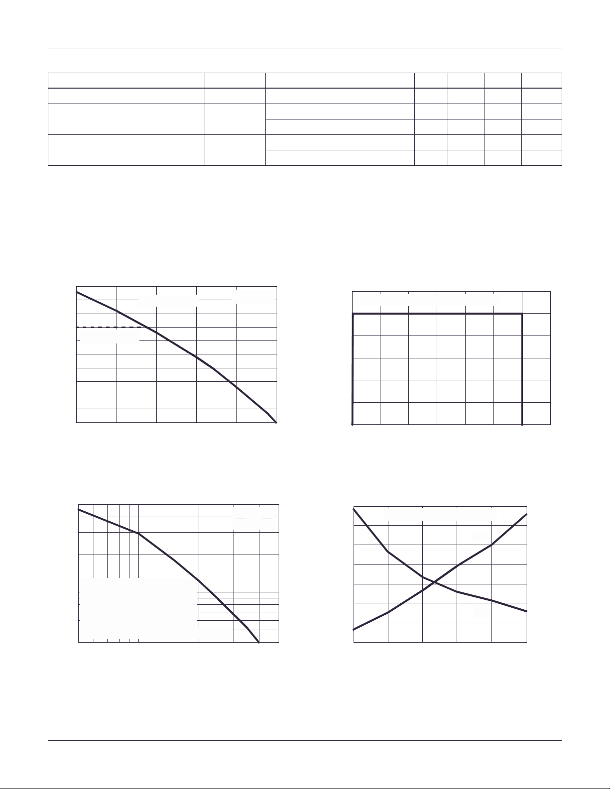
Typical Performance Curves Unless Otherwise Specified
100
80
PACKAGE LIMIT
60
DIE CAPABILITY
V
= 15V
GE
120
TJ = 150oC, RG = 3Ω, V
100
80
o
C/W
o
C/W
is the turn-on loss of the IGBT only. E
ON1
as the IGBT. The di ode type is speci fied in
J
= 15V, L = 100µH
GE
ON2
40
20
, DC COLLECTOR CURRENT (A)
CE
I
0
25 75 100 125 150
50
TC, CASE TEMPERATURE (oC)
FIGURE 1. DC COLLECT OR CURRENT vs CASE
TEMPERATURE
500
300
f
= 0.05 / (t
MAX1
= (PD - PC) / (E
f
100
MAX2
= CONDUCTION DISSIPATION
P
C
(DUTY FACTOR = 50%)
, OPERATING FREQUENCY (kHz)
R
= 0.43oC/W, SEE NOTES
ØJC
MAX
f
TJ = 125oC, RG = 3Ω, L = 500µH, V
40
5
I
d(OFF)I
, COLLECTOR TO EMITTER CURRENT (A)
CE
+ t
ON2
d(ON)I
+ E
OFF
)
)
= 390V
CE
TCV
75
60
40
20
, COLLECTOR TO EMITTER CURRENT (A)
0
CE
I
0
VCE, COLLECTOR TO EMITTER VOLT AGE (V)
300 400200100 500 600
700
FIGURE 2. MINIMUM SWITCHING SAFE OPERATING AREA
GE
o
C
15V
5010 20
4030
12
10
8
6
4
2
, SHORT CIRCUIT WITHSTAND TIME (µs)
0
SC
t
10 11 12 15
VCE = 390V, RG = 3Ω, TJ = 125oC
I
SC
t
SC
13 14
VGE, GATE TO EMITTER VOLTAGE (V)
45014
400
350
300
250
200
150
100
, PEAK SHORT CIRCUIT CURRENT (A)
SC
I
FIGURE 3. OPERATING FREQUENCY vs COLLECTOR T O
FIGURE 4. SHORT CIRCUIT WITHSTAND TIME
EMITTER CURRENT
©2002 Fairchild Semiconductor Corporation HGTG20N60A4D, HGT4E20N60A4DS Rev. C
 Loading...