

Fairchild Semiconductor HGTP7N60A4D, HGTG7N60A4D, HGT1S7N60A4DS Datasheet
HGTG7N60A4D, HGTP7N60A4D,
Data Sheet December 2001
HGT1S7N60A4DS
600V, SMPS Series N-Channel IGBT with
Anti-Parallel Hyperfast Diode
The HGTG7N60A4D, HGTP7N60A4D and
HGT1S7N60A4DS are MOS gated high voltage switching
devices combining the best features of MO SFETs and
bipolar transistors. These devices have the high input
impedance of a MOSFET and the low on-state conduction
loss of a bipolar transistor. The much lower on-state voltage
drop varies only moderately between 25
o
C and 150oC. The
IGBT used is the devel opm ent type T A 49 331 . The diod e
used in anti-par al lel is the developme nt typ e TA4937 0.
This IGBT is ideal for many high voltage switchin g
applications operating at high frequencies where low
conduction losses are essential. This device has been
optimized for high frequency switch mode power
supplies.
Formerly Developmental Type TA49333.
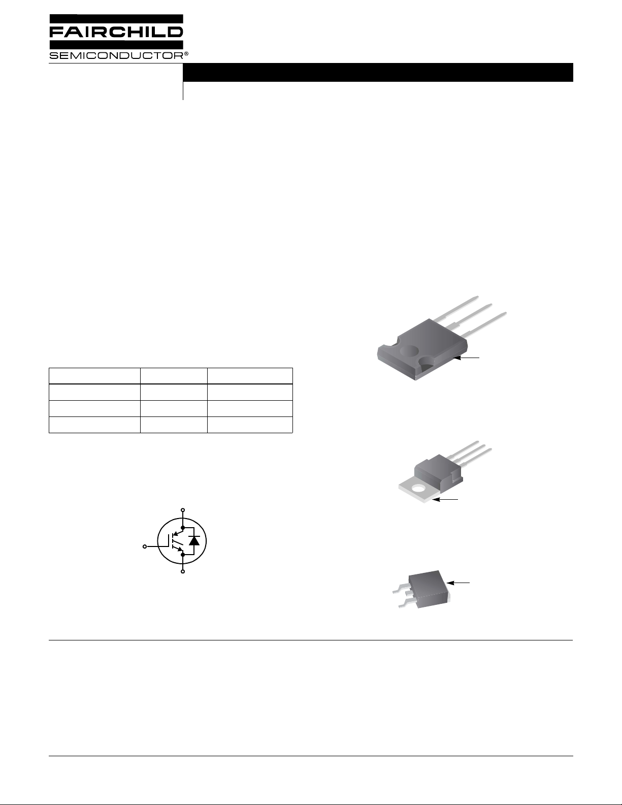
Ordering Information
PART NUMBER PACKAGE BRAND
HGTG7N60A4D TO-247 7N60A4D
HGTP7N60A4D TO-220AB 7N60A4D
HGT1S7N60A4DS TO-263AB 7N60A4D
NOTE: When ordering, use the entire part number. Add the suffix 9A
to obtain the TO-263AB variant in tape and reel, e.g.,
HGT1S7N60A4DS9A.
Features
• >100kHz Operation At 390V, 7A
• 200kHz Operation At 390V, 5A
• 600V Switching SOA Capability
• Typical Fall Time. . . . . . . . . . . . . . . . . 75ns at T
• Low Conduction Loss
• Temperature Compensating SABER™ Model
www.fairchildsemi.com
Packaging
JEDEC STYLE TO-247
E
C
G
COLLECTOR
(FLANGE)
JEDEC TO-220AB
E
C
G
= 125oC
J
Symbol
C
G
E
G
FAIRCHILD SEMICONDUCTOR IGBT PRODUCT IS COVERED BY ONE OR MORE OF THE FOLLOWING U.S. PATENTS
4,364,073 4,417,385 4,430,792 4,443,931 4,466,176 4,516,143 4,532,534 4,587,713
4,598,461 4,605,948 4,620,211 4,631,564 4,639,754 4,639,762 4,641,162 4,644,637
4,682,195 4,684,413 4,694,313 4,717,679 4,743,952 4,783,690 4,794,432 4,801,986
4,803,533 4,809,045 4,809,047 4,810,665 4,823,176 4,837,606 4,860,080 4,883,767
4,888,627 4,890,143 4,901,127 4,904,609 4,933,740 4,963,951 4,969,027
©2001 Fairchild Semiconductor Corpo ration HGTG7N60A4D, HGTP7N60A4D, HGT1S7N60A4DS Rev. B
JEDEC TO-263AB
E
COLLECTOR
(FLANGE)
COLLECTOR
(FLANGE)
HGTG7N60A4D, HGTP7N60A4D, HGT1S7N60A4DS
Absolute Maximum Ratings
TC = 25oC, Unless Otherwise Specified
ALL TYPES UNITS
Collector to Emitter Voltage . . . . . . . . . . . . . . . . . . . . . . . . . . . . . . . . . . . . . . . . . . . . . . . . . BV
CES
600 V
Collector Current Continuous
= 25oC . . . . . . . . . . . . . . . . . . . . . . . . . . . . . . . . . . . . . . . . . . . . . . . . . . . . . . . . . . . . I
At T
C
= 110oC . . . . . . . . . . . . . . . . . . . . . . . . . . . . . . . . . . . . . . . . . . . . . . . . . . . . . . . . . . I
At T
C
Collector Current Pulsed (Note 1) . . . . . . . . . . . . . . . . . . . . . . . . . . . . . . . . . . . . . . . . . . . . . . . I
Gate to Emitter Voltage Continuous. . . . . . . . . . . . . . . . . . . . . . . . . . . . . . . . . . . . . . . . . . . . V
Gate to Emitter Voltage Pulsed . . . . . . . . . . . . . . . . . . . . . . . . . . . . . . . . . . . . . . . . . . . . . . . V
Switching Safe Operating Area at T
Pow er Dissi pation Total at T
C
Power Dissipation Derating T
= 150oC, Figure 2 . . . . . . . . . . . . . . . . . . . . . . . . . . . . SSOA 35A at 600V
J
= 25oC . . . . . . . . . . . . . . . . . . . . . . . . . . . . . . . . . . . . . . . . . . . . P
> 25oC . . . . . . . . . . . . . . . . . . . . . . . . . . . . . . . . . . . . . . . . . . . . . . 1.0 W/oC
C
Operating and Storage Junction Temperature Range . . . . . . . . . . . . . . . . . . . . . . . . . . . T
C25
C110
CM
GES
GEM
D
, T
J
STG
Maximum Lead T emperature f or Soldering
Leads at 0.063in (1.6mm) from Case for 10s. . . . . . . . . . . . . . . . . . . . . . . . . . . . . . . . . . . . . . T
Package Body for 10s, See Tech Brief 334 . . . . . . . . . . . . . . . . . . . . . . . . . . . . . . . . . . . . T
CAUTION: Stresses above those listed in “A bsolute Maximu m Rating s” may cause per manent d amage to t he device. This is a str ess on ly rating and operation o f the
device at these or any other conditions above those indicated in the operational sections of this specification is not implied.
L
PKG
34 A
14 A
56 A
±20 V
±30 V
125 W
-55 to 150
300
260
o
C
o
C
o
C
NOTE:
1. Pulse width limited by maximum junction temperature.
Electrical Specifications
TJ = 25oC, Unless Otherwise Specified
PARAMETER SYMBOL TEST CONDITIONS MIN TYP MAX UNITS
Collector to Emitter Breakdown Voltage BV
Collector to Emitter Leakage Current I
Collector to Emitter Saturation Voltage V
Gate to Emitter Threshold Voltage V
Gate to Emitter Leakage Current I
CES
CES
CE(SAT)IC
GE(TH)
GES
Switching SOA SSOA T
Gate to Emitter Plateau Voltage V
On-State Gate Charge Q
Current Turn-On Delay Time t
Current Rise Time t
Current Turn-Off Delay Time t
Current Fall Time t
Turn-On Energy E
Turn-On Energy E
Turn-Off Energy (Note 2) E
Current Turn-On Delay Time t
Current Rise Time t
Current Turn-Off Delay Time t
Current Fall Time t
Turn-On Energy (Note 2) E
Turn-On Energy (Note 2) E
Turn-Off Energy (Note 3) E
GEP
g(ON)
d(ON)I
rI
d(OFF)I
fI
ON1
ON2
OFF
d(ON)I
rI
d(OFF)I
fI
ON1
ON2
OFF
IC = 250µA, VGE = 0V 600 - - V
VCE = 600V TJ = 25oC - - 250 µA
T
= 125oC--2mA
J
V
GE
= 7A,
= 15V
T
= 25oC-1.92.7V
J
T
= 125oC-1.62.2V
J
IC = 250µA, VCE = 600V 4.5 5.9 7 V
VGE = ±20V - - ±250 nA
= 150oC, RG = 25Ω, VGE = 15V,
J
L = 100µH, V
= 600V
CE
35 - - A
IC = 7A, VCE = 300V - 9 - V
IC = 7A,
= 300V
V
CE
IGBT and Diode at TJ = 25oC,
= 7A,
I
CE
V
= 390V,
CE
= 15V,
V
GE
= 25Ω,
R
G
L = 1mH,
Test Circuit (Figure 24)
V
= 15V - 37 45 nC
GE
V
= 20V - 48 60 nC
GE
-11- ns
-11- ns
- 100 - ns
-45- ns
-55- µJ
- 120 150 µJ
-6075µJ
IGBT and Diode at TJ = 125oC,
= 7A,
I
CE
V
= 390V, VGE = 15V,
CE
= 25Ω,
R
G
L = 1mH,
Test Circuit (Figure 24)
-10- ns
-7-ns
- 130 150 ns
-7585ns
-50- µJ
- 200 215 µJ
- 125 170 µJ
©2001 Fairchild Semiconductor Corpo ration HGTG7N60A4D, HGTP7N60A4D, HGT1S7N60A4DS Rev. B
0
)
0
HGTG7N60A4D, HGTP7N60A4D, HGT1S7N60A4DS
Electrical Specifications
TJ = 25oC, Unless Otherwise Specified (Continued)
PARAMETER SYMBOL TEST CONDITIONS MIN TYP MAX UNITS
Diode Forward Voltage V
Diode Reverse Recovery Time t
Thermal Resistance Junction To Case R
EC
rr
θJC
IEC = 7A - 2.4 - V
IEC = 7A, dIEC/dt = 200A/µs-34-ns
I
= 1A, dIEC/dt = 200A/µs-22-ns
EC
IGBT - - 1.0
Diode - - 2.2
NOTES:
2. Values for two Turn-On loss conditions are shown for the convenience of the circuit designer. E
is the turn-on loss when a typical diode is used in the test circuit and the diode is at the same T
Figure 24.
3. Turn-Off Energy Loss (E
at the point where the collector current equals zero (I
of Power Device Turn-Off Switching Loss. This test method produces the true total Turn-Off Energy Loss.
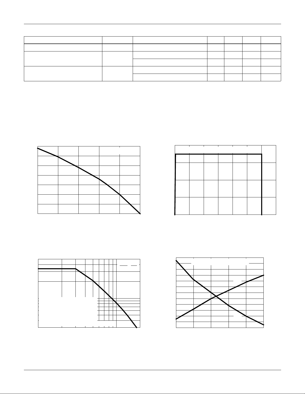
Typical Performance Curves
35
30
25
20
15
) is defined as the integral of the instantaneous power loss starting at the trailing edge of the input pulse and ending
OFF
= 0A). All devices were tested per JEDEC Standard No. 24-1 Method for Measurement
CE
Unless Otherwise Specified
40
V
= 15V
GE
TJ = 150oC, RG = 25Ω, V
30
20
o
C/W
o
C/W
is the turn-on loss of the IGBT only. E
ON1
as the IGBT. The diode type is specified in
J
= 15V, L = 100µH
GE
ON2
10
, DC COLLECTOR CURRENT (A)
5
CE
I
0
25 75 100 125 15
50
TC, CASE TEMPERATURE (oC)
FIGURE 1. DC COLLECTOR CURRENT vs CASE
10
, COLLECTOR TO EMITTER CURRENT (A
CE
0
I
0
VCE, COLLECTOR TO EMITTER VOLTAGE (V)
300 400200100 500 600
FIGURE 2. MINIMUM SWITCHING SAFE OPERATING AREA
700
TEMPERATURE
500
200
100
f
= 0.05 / (t
MAX1
= (PD - PC) / (E
f
MAX2
= CONDUCTION DISSIPATION
P
C
, OPERATING FREQUENCY (kHz)
MAX
f
30
(DUTY FACTOR = 50%)
= 1.0oC/W, SEE NOTES
R
ØJC
TJ = 125oC, RG = 25Ω, L = 1mH, V
1
, COLLECTOR TO EMITTER CURRENT (A)
I
CE
d(OFF)I
+ t
ON2
)
d(ON)I
+ E
)
OFF
= 390V
CE
510
TCV
o
75
GE
15V
C
2
14
12
10
8
6
, SHORT CIRCUIT WITHSTAND TIME (µs)
SC
4
t
10 11 12 15
VCE = 390V, RG = 25Ω, TJ = 125oC
I
SC
t
SC
13 14
VGE, GATE TO EMITTER VOLTAGE (V)
14016
120
100
80
60
40
20
, PEAK SHORT CIRCUIT CURRENT (A)
SC
I
FIGURE 3. OPERATING FREQUENCY vs COLLECT OR TO
FIGURE 4. SHORT CIRCUIT WITHSTAND TIME
EMITTER CURRENT
©2001 Fairchild Semiconductor Corpo ration HGTG7N60A4D, HGTP7N60A4D, HGT1S7N60A4DS Rev. B
 Loading...