

Fairchild Semiconductor HGT1S20N60C3S Datasheet
HGTG20N60C3, HGTP20N60C3,
Data Sheet December 2001
HGT1S20N60C3S
45A, 600V, UFS Series N-Channel IGBT
This family of MOS gated high voltage switching devices
combining the best features of MOSFETs and bipolar
transistors . These devices ha ve the high i npu t impe dance of
a MOSFET and the low on-s tate con duction lo ss of a bi polar
transistor. The much lower on-state voltage drop varies only
moderately bet w e en 25
o
C and 150oC.
The IGBT is ideal for many high voltage switc hi ng
applications operating at moderate freq ue ncies where low
conduction losses are ess ential, such as: AC and DC motor
controls, power supplies and drivers for solenoids, relays
and contactors.
Formerly developmental type TA49178.
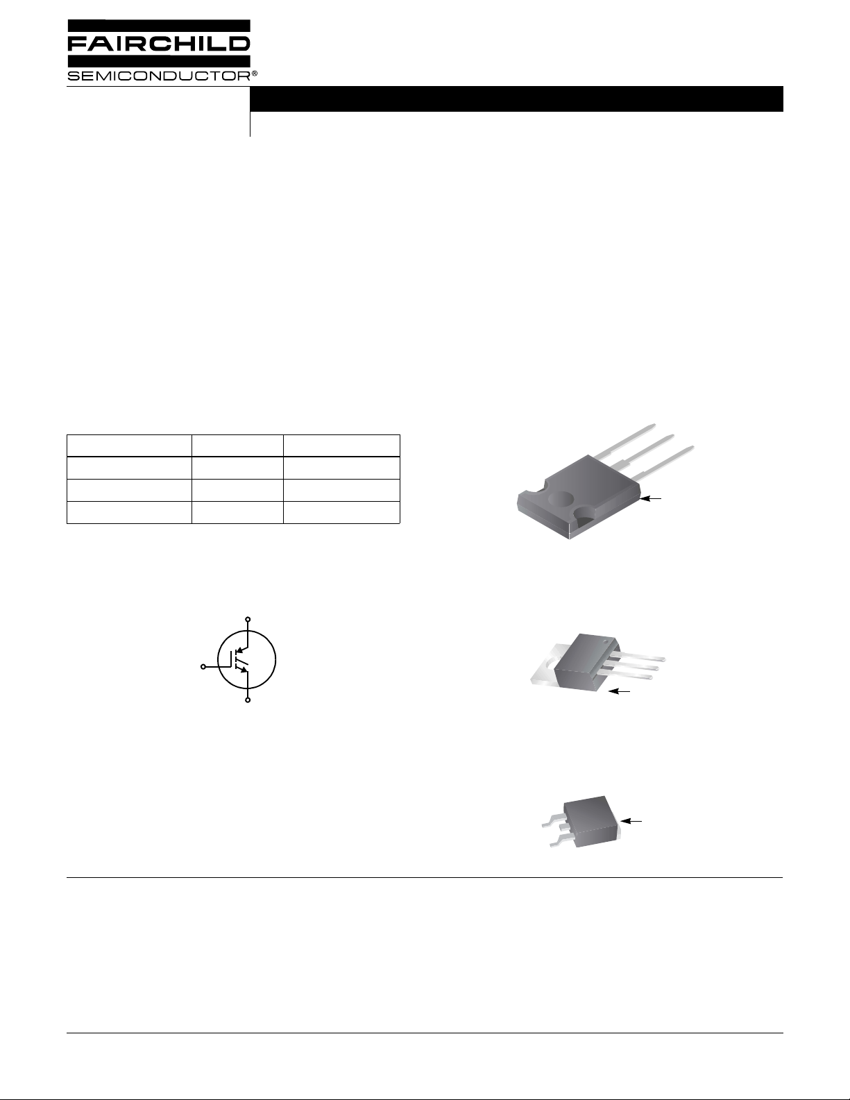
Ordering Information
PART NUMBER PACKAGE BRAND
HGTG20N60C3 TO-247 G20N60C3
HGTP20N60C3 TO-220AB G20N60C3
HGT1S20N60C3S TO-263AB G20N60C3
NOTE: When ordering, use the entire part number. Add the suffix 9A
to obtain the TO-263AB variant in the tape and reel, i.e.,
HGT1S20N60C3S9A.
Features
• 45A, 600V, TC = 25oC
• 600V Switching SOA Capability
• Typical Fall Time. . . . . . . . . . . . . . . . 108ns at T
• Short Circuit Rating
• Low Conduction Loss
• Related Literature
- TB334 “Guidelines f or Solde ring Surface Mount
Components to PC Boards”
Packaging
JEDEC STYLE TO-247
E
C
G
COLLECTOR
(FLANGE)
= 150oC
J
Symbol
C
G
E
INTERSIL CORPORATION IGBT PRODUCT IS COVERED BY ONE OR MORE OF THE FOLLOWING U.S. PATENTS
4,364,073 4,417,385 4,430,792 4,443,931 4,466,176 4,516,143 4,532,534 4,587,713
4,598,461 4,605,948 4,620,211 4,631,564 4,639,754 4,639,762 4,641,162 4,644,637
4,682,195 4,684,413 4,694,313 4,717,679 4,743,952 4,783,690 4,794,432 4,801,986
4,803,533 4,809,045 4,809,047 4,810,665 4,823,176 4,837,606 4,860,080 4,883,767
4,888,627 4,890,143 4,901,127 4,904,609 4,933,740 4,963,951 4,969,027
JEDEC TO-220AB (ALTERNATE VERSION)
E
C
G
COLLECTOR
(FLANGE)
JEDEC TO-263AB
G
E
COLLECTOR
(FLANGE)
©2001 Fairchild Semiconductor Corpo ration HGTG20N60C3, HGTP20N60C3, HGT1S20N60C3S Rev. B
HGTG20N60C3, HGTP20N60C3, HGT1S20N60C 3S
Absolute Maximum Ratings
TC = 25oC, Unless Otherwise Specified
ALL TYPES UNITS
Collector to Emitter Voltage . . . . . . . . . . . . . . . . . . . . . . . . . . . . . . . . . . . . . . . . . . . . . . BV
CES
600 V
Collector Current Continuous
= 25oC . . . . . . . . . . . . . . . . . . . . . . . . . . . . . . . . . . . . . . . . . . . . . . . . . . . . . . . . . I
At T
C
= 110oC . . . . . . . . . . . . . . . . . . . . . . . . . . . . . . . . . . . . . . . . . . . . . . . . . . . . . . . I
At T
C
Collector Current Pulsed (Note 1) . . . . . . . . . . . . . . . . . . . . . . . . . . . . . . . . . . . . . . . . . . . I
Gate to Emitter Voltage Continuous. . . . . . . . . . . . . . . . . . . . . . . . . . . . . . . . . . . . . . . . . V
Gate to Emitter Voltage Pulsed . . . . . . . . . . . . . . . . . . . . . . . . . . . . . . . . . . . . . . . . . . . . V
Switching Safe Operating Area at T
Pow er Dissi pation Total at T
C
Power Dissipation Derating T
= 150oC (Figure 2) . . . . . . . . . . . . . . . . . . . . . . . SSOA 20A at 600V
J
= 25oC . . . . . . . . . . . . . . . . . . . . . . . . . . . . . . . . . . . . . . . . . P
> 25oC . . . . . . . . . . . . . . . . . . . . . . . . . . . . . . . . . . . . . . . . . . 1.32 W/oC
C
Reverse Voltage Avalanche Energy. . . . . . . . . . . . . . . . . . . . . . . . . . . . . . . . . . . . . . . . . E
Operating and Storage Junction Temperature Range . . . . . . . . . . . . . . . . . . . . . . . . T
C25
C110
CM
GES
GEM
D
ARV
, T
J
STG
Maximum Temperature for Soldering
Leads at 0.063in (1.6mm) from Case for 10s. . . . . . . . . . . . . . . . . . . . . . . . . . . . . . . . . . T
Package Body for 10s, see Tech Brief 334. . . . . . . . . . . . . . . . . . . . . . . . . . . . . . . . . . . T
Short Circuit Withstand Time (Not e 2) at V
Short Circuit Withstand Time (Not e 2) at V
CAUTION: Stresses above those listed in “A bsolute Maximu m Rating s” may cause per manent d amage to t he device. This is a str ess on ly rating and operation o f the
device at these or any other conditions above those indicated in the operational sections of this specification is not implied.
= 12V. . . . . . . . . . . . . . . . . . . . . . . . . . . . . .t
GE
= 10V. . . . . . . . . . . . . . . . . . . . . . . . . . . . . .t
GE
L
pkg
SC
SC
45 A
20 A
300 A
±20 V
±30 V
164 W
100 mJ
-55 to 150
300
260
4 µs
10 µs
o
C
o
C
o
C
NOTES:
1. Pulse width limited by maximum junction temperature.
2. V
= 360V, TJ = 125oC, RG = 10Ω.
CE(PK)
Electrical Specifications
TC = 25oC, Unless Otherwise Specified
PARAMETER SYMBOL TEST CONDITIONS MIN TYP MAX UNITS
Collector to Emitter Breakdown Voltage BV
Emitter to Collector Breakdown Voltage BV
Collector to Emitter Leakage Current I
Collector to Emitter Saturation Voltage V
Gate to Emitter Threshold Voltage V
Gate to Emitter Leakage Current I
CES
ECS
CES
CE(SAT)IC
GE(TH)
GES
Switching SOA SSOA T
Gate to Emitter Plateau Voltage V
On-State Gate Charge Q
Current Turn-On Delay Time t
Current Rise Time t
Current Turn-Off Delay Time t
Current Fall Time t
Turn-On Energy (Note 4) E
Turn-On Energy (Note 4) E
Turn-Off Energy (Note 3) E
GEP
G(ON)
d(ON)I
rI
d(OFF)I
fI
ON1
ON2
OFF
IC = 250µA, VGE = 0V 600 - - V
IC = 10mA, VGE = 0V 15 28 - V
VCE = BV
V
= I
GE
C110
= 15V
CES
IC = 250µA, VCE = V
TC = 25oC - - 250 µA
= 150oC--5.0mA
T
C
T
= 25oC-1.41.8V
C
T
= 150oC-1.51.9V
C
GE
3.4 4.8 6.3 V
VGE = ±20V - - ±250 nA
= 150oC, RG =
J
10Ω, V
L = 100µH
ICE = I
ICE = I
= 15V,
GE
, VCE = 0.5 BV
C110
C110
VCE = 0.5 BV
IGBT and Diode at TJ = 25oC
= I
I
CE
C110
VCE = 0.8 BV
VGE = 15V
R
= 10Ω
G
L = 1mH
Test Circuit (Figure 17)
V
= 480V 120 - - A
CE
= 600V 20 - - A
V
CE
CES
-8.4- V
VGE = 15V - 91 110 nC
CES
= 20V - 122 145 nC
V
GE
-2832ns
-2428ns
CES
- 151 210 ns
-5598ns
- 295 320 µJ
- 500 550 µJ
- 500 700 µJ
©2001 Fairchild Semiconductor Corpo ration HGTG20N60C3, HGTP20N60C3, HGT1S20N60C3S Rev. B
HGTG20N60C3, HGTP20N60C3, HGT1S20N60C 3S
Electrical Specifications
TC = 25oC, Unless Otherwise Specified (Continued)
PARAMETER SYMBOL TEST CONDITIONS MIN TYP MAX UNITS
Current Turn-On Delay Time t
d(ON)I
Current Rise Time t
Current Turn-Off Delay Time t
d(OFF)I
Current Fall Time t
Turn-On Energy (Note 4) E
Turn-On Energy (Note 4) E
Turn-Off Energy (Note 3) E
Thermal Resistance Junction To Case R
rI
fI
ON1
ON2
OFF
θJC
IGBT and Diode at TJ = 150oC
I
= I
CE
C110
VCE = 0.8 BV
VGE = 15V
R
= 10Ω
G
CES
L = 1mH
Test Circuit (Figure 17)
NOTES:
3. T urn-Off Energy Loss (E
at the point where the collector current equals zero (I
) is defined as the integral of the instantaneous po wer loss starting at the trailing edge of the input pulse and ending
OFF
= 0A). All devices were tested per JEDEC Standard No. 24-1 Method for Measurement
CE
of Pow er De vice Turn-Off Switching Loss. This test method produces the true total Turn-Off Energy Loss.
4. Values for two T urn-On loss conditions are shown for the convenience of the circuit des igner. E
turn-on loss when a typical diode i s u s ed i n the t est circu it and the diode is at the same T
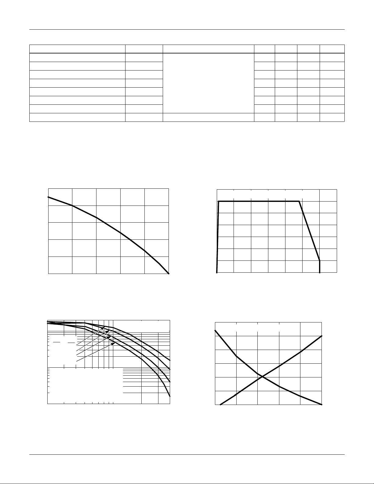
Typical Performance Curves
50
40
30
Unless Otherwise Specified
= 15V
V
GE
140
TJ = 150oC, RG = 10Ω, V
120
100
80
J
is the turn-on loss of the IGBT only. E
ON1
as the IGBT. The diode type is specified in Figure 17.
-2832ns
-2428ns
- 280 450 ns
- 108 210 ns
- 380 410 µJ
-1.01.1mJ
-1.21.7mJ
ON2
o
C/W
is the
- - 0.76
= 15V, L = 100µH
GE
20
10
, DC COLLECTOR CURRENT (A)
CE
I
0
25 75 100 125 150
50
TC, CASE TEMPERATURE (oC)
FIGURE 1. DC COLLECTOR CURRENT vs CASE
TEMPERATURE
TJ = 150oC, RG = 10Ω,
, OPERATING FREQUENCY (kHz)
MAX
f
100
10
T
V
C
GE
o
75
C
15V
o
C
75
10V
o
110
C
15V
110oC
10V
f
= 0.05 / (t
MAX1
f
= (PD - PC) / (E
MAX2
= CONDUCTION DISSIPATION
P
C
(DUTY FACTOR = 50%)
R
= 0.76oC/W, SEE NOTES
ØJC
1
2
I
CE
d(OFF)I
5
, COLLECTOR TO EMITTER CURRENT (A)
+ t
ON2
d(ON)I
+ E
OFF
L = 1mH, V
)
)
CE
= 480V
60
40
20
, COLLECTOR TO EMITTER CURRENT (A)
0
CE
I
0
VCE, COLLECTOR TO EMITTER VOLTAGE (V)
300 400200100 500 600
700
FIGURE 2. MINIMUM SWITCHING SAFE OPERATING AREA
14
VCE = 360V, RG = 10Ω, TJ = 125oC
12
10
8
6
4
, SHORT CIRCUIT WITHSTAND TIME (µs)
2
SC
4010 20
t
10 11 12 13 14 15
VGE, GATE TO EMITTER VOLTAGE (V)
I
SC
450
400
350
300
250
200
t
SC
150
, PEAK SHORT CIRCUIT CURRENT (A)
SC
I
FIGURE 3. OPERATING FREQUENCY vs COLLECT OR TO
FIGURE 4. SHORT CIRCUIT WITHSTAND TIME
EMITTER CURRENT
©2001 Fairchild Semiconductor Corpo ration HGTG20N60C3, HGTP20N60C3, HGT1S20N60C3S Rev. B
 Loading...