

Fairchild Semiconductor FST3244WMX, FST3244WM, FST3244QSCX, FST3244QSC, FST3244MTCX Datasheet
...
© 1999 Fairchild Semiconductor Corporation DS500021 www.fairchildsemi.com
June 1997
Revised December 1999
FST3244 Octal Bus Switch
FST3244
Octal Bus Switch
General Description
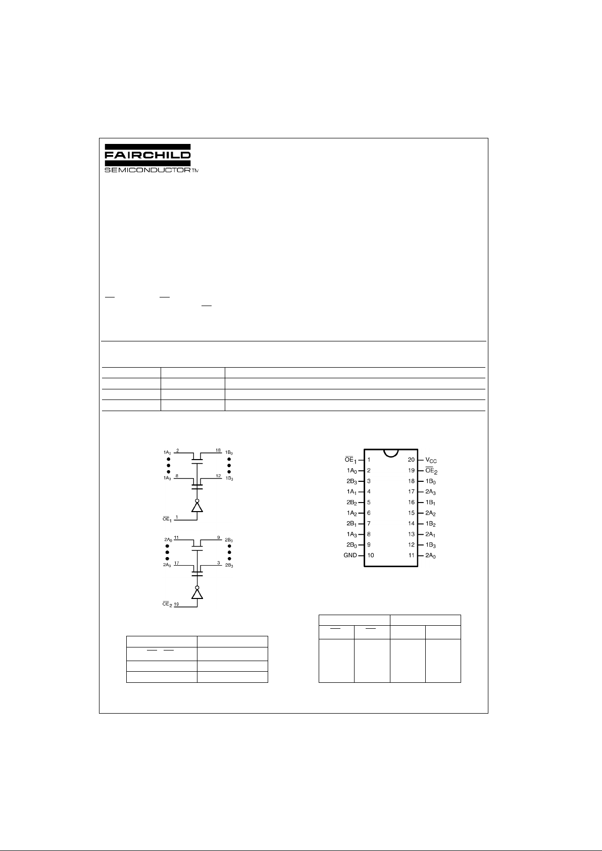
The Fairchild Switch FST3244 provides 8-bits of highspeed CMOS TTL-compati ble bus switch ing in a standa rd
’244 pin-out. The low on resi stance of the switch allows
inputs to be connect ed to output s with out ad ding propag ation delay or generating additional ground bounce noise.
The device is organized as two 4-bit switches with separate
OE
inputs. When OE is LOW, the switch is ON and Port A
is connected to Port B. When OE
is HIGH, the switch is
OPEN and a high- impe dan ce sta t e exist s b etwe en th e tw o
ports.
Features
■ 4Ω switch connection between two ports.
■ Minimal propagation delay through the switch.
■ Low l
CC
.
■ Zero bounce in flow-through mode.
■ Control inputs compatible with TTL level.
Ordering Code:
Devices also availab le in Tape and Reel. Specify by appending th e s uffix let t er “X” to the ordering code.
Logic Diagram
Pin Descriptions
Connection Diagram
Truth T able
Order Number Package Number Package Description
FST3244WM M20B 20-Lead Small Outline Integrated Circuit (SOIC), JEDEC MS-013, 0.300 Wide
FST3244QSC MQA20 20-Lead Quarter Size Outline Package (QSOP), JEDEC MO-137, 0.150 Wide
FST3244MTC MTC20 20-Lead Thin Shrink Small Outline Package (TSSOP), JEDEC MO-153, 4.4mm Wide
Pin Name Description
OE
1
, OE
2
Bus Switch Enable
1A, 2A Bus A
1B, 2B Bus B
Inputs Inputs/Outputs
OE
1
OE
2
1A, 1B 2A, 2B
LL1A = 1B 2A = 2B
LH1A = 1B Z
HLZ2A = 2B
HHZZ
www.fairchildsemi.com 2
FST3244
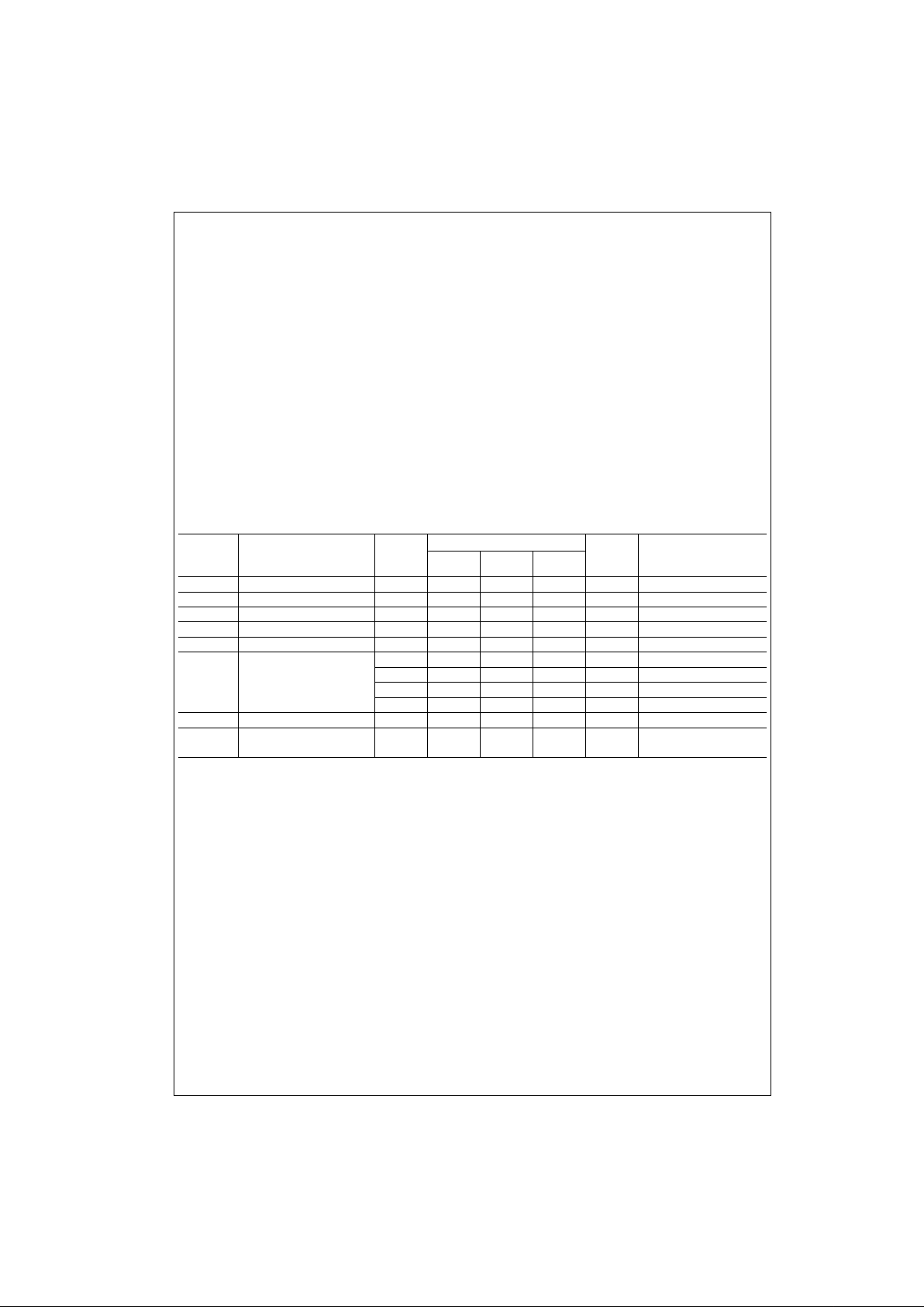
Absolute Maximum Ratings(Note 1) Recommended Operating
Conditions
(Note 3)
Note 1: The Absolute Maximum Ratings are those values beyond which
the safety of the dev ice cannot be guaranteed. T he device sh ould not be
operated at these limits. The parametric values defined in the Electrical
Characteristics tables are not guaranteed at the absolute maximum rating.
The Recommende d Opera ting Condit ions table s will de fine the co nditions
for actual device operation.
Note 2: The input and output negative volt age ratin gs may be exceede d if
the input and output diode current ratings are observed.
Note 3: Unused control inputs m ust be held HIGH o r LOW. They may no t
float.
DC Electrical Characteristics
Note 4: Typical values are at VCC = 5.0V and TA = +25°C
Note 5: Measured by th e v olt age drop between A and B pins at the indicated c urrent through the switc h. On resistance is det erm ined by the lower of the
voltages on the two (A or B) pins.
Supply Voltage (VCC) −0.5V to +7.0V
DC Switch Voltage (V
S
) −0.5V to +7.0V
DC Input Voltage (V
IN
) (Note 2) −0.5V to +7.0V
DC Input Diode Current (l
IK
) VIN<0V −50mA
DC Output (I
OUT
) Sink Current 128mA
DC V
CC
/GND Current (ICC/I
GND
) +/− 100mA
Storage Temperature Range (T
STG
) −65°C to +150 °C
Power Supply Operating (V
CC
) 4.0V to 5.5V
Input Voltage (V
IN
)0V to 5.5V
Output Voltage (V
OUT
)0V to 5.5V
Input Rise and Fall Time (t
r
, tf)
Switch Control Input 0nS/V to 5nS/V
Switch I/O 0nS/V to DC
Free Air Operating Temperature (T
A
) −40 °C to +85 °C
Symbol Parameter
V
CC
(V)
TA = −40 °C to +85 °C
Units Conditions
Min
Typ
(Note 4)
Max
V
IK
Clamp Diode Voltage 4.5 −1.2 V IIN = −18mA
V
IH
High Level Input Voltage 4.0–5.5 2.0 V
V
IL
Low Level Input Voltage 4.0–5.5 0.8 V
I
I
Input Leakage Current 5.5 ±1.0 µA0≤ VIN ≤5.5V
I
OZ
OFF-STATE Leakage Current 5.5 ±1.0 µA0 ≤A, B ≤V
CC
R
ON
Switch On Resistance 4.5 4 7 Ω VIN = 0V, IIN = 64mA
(Note 5) 4.5 4 7 Ω VIN = 0V, IIN = 30mA
4.5 8 15 Ω VIN = 2.4V, IIN = 15mA
4.0 11 20 Ω VIN = 2.4V, IIN = 15mA
I
CC
Quiescent Supply Current 5.5 3 µAVIN = VCC or GND, I
OUT
= 0
∆ I
CC
Increase in I
CC
per Input 5.5 2.5 mA One input at 3.4V
Other inputs at VCC or GND
 Loading...