

Fairchild Semiconductor FST3126QSCX, FST3126MX, FST3126MTCX, FST3126M, FST3126CW Datasheet
© 1999 Fairchild Semiconductor Corporation DS500044 www.fairchildsemi.com
August 1997
Revised December 1999
FST3126 Quad Bus Switch
FST3126
Quad Bus Switch
General Description
The Fairchild Switch FST3126 provides four high-speed
CMOS TTL-compatible bus switches. The low on resistance of the switch allows inputs to be connect ed to outputs without adding propagation delay or generating
additional ground bounce noise.
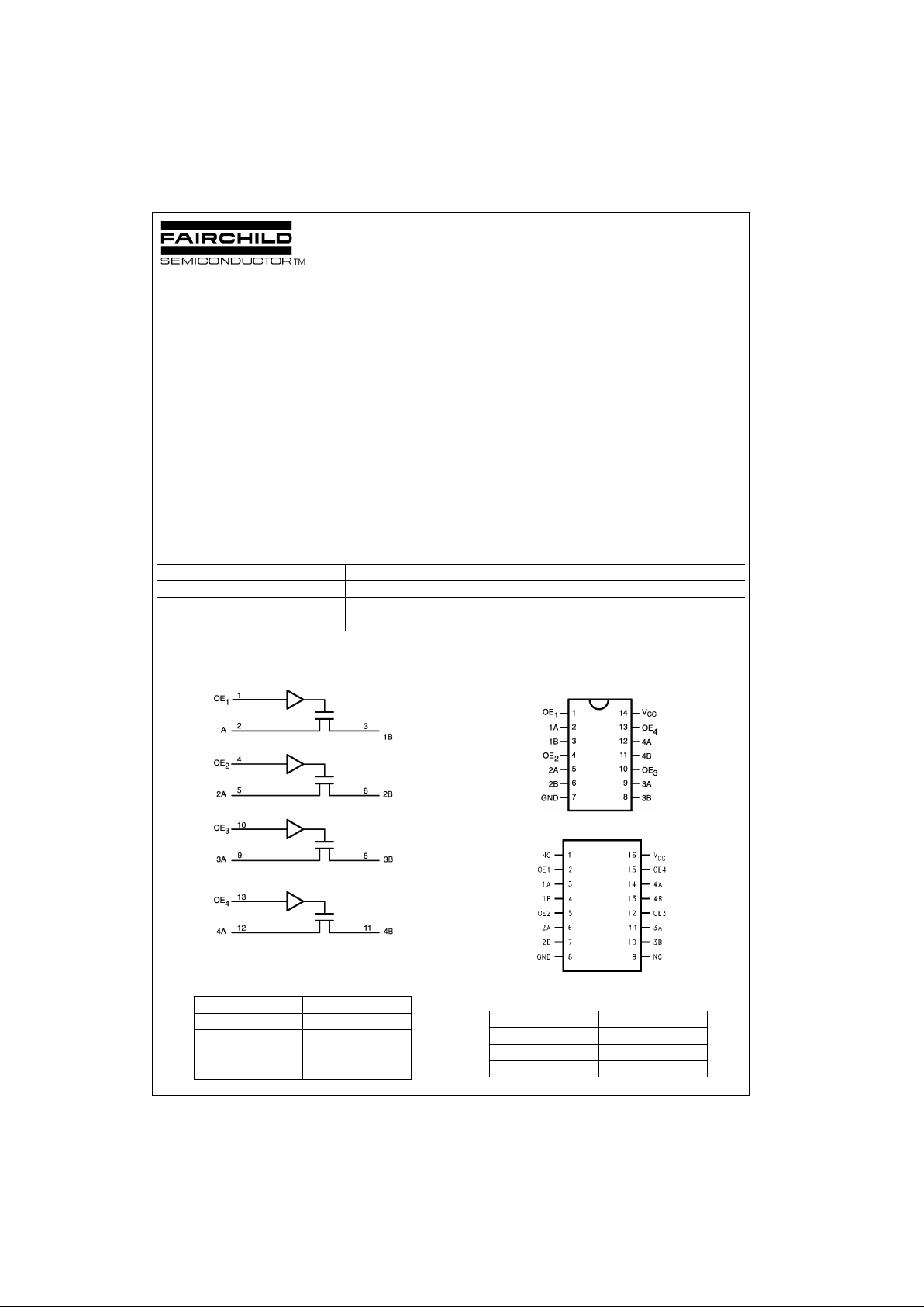
The device is organized as four 1- bit switches with separate OE inputs. When OE is HIGH, the switch is ON and
Port A is connected to Port B. When OE is LOW, the switch
is OPEN and a high-impedan ce state exists between the
two ports.
Features
■ 4Ω switch connection between two ports.
■ Minimal propagation delay through the switch.
■ Low l
CC
.
■ Zero bounce in flow-through mode.
■ Control inputs compatible with TTL level.
Ordering Code:
Devices also availab le in Tape and Reel. Specify by appending the s uffix let te r “X” to the ordering code.
Logic Diagram
Pin Descriptions
Connection Diagrams
Pin Assignment for S OIC and TSSOP
Pin Assignment for QSOP
Truth T able
Order Number Package Number Package Description
FST3126M M14A 14-Lead Small Outline Integrated Circuit (SOIC), JEDEC MS-120, 0.150 Narrow
FST3126QSC MQA16 16-Lead Quarter Size Outline Package (QSOP), JEDEC MO-137, 0.150 Wide
FST3126MTC MTC14 14-Lead Thin Shrink Small Outline Package (TSSOP), JEDEC MO-153, 4.4mm Wide
Pin Name Description
OE
1
, OE2, OE3, OE4Bus Switch Enables
1A, 2A, 3A, 4A Bus A
1B, 2B, 3B, 4B Bus B
NC Not Connected
Inputs Inputs/Outputs
OE A,B
LZ
HA = B
www.fairchildsemi.com 2
FST3126
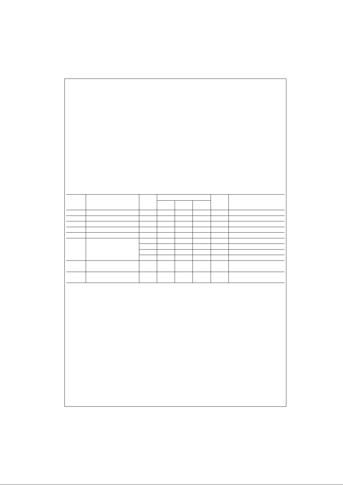
Absolute Maximum Ratings(Note 1) Recommended Operating
Conditions
(Note 3)
Note 1: The “Absolute Maximum Ratings” are those values beyon d which
the safety of the dev ice cannot be guaranteed. T he device sh ould not be
operated at these limit s. The parametric values defin ed in the Electrical
Characteristics tables are not guaranteed at the absolute maximum rating.
The “Recomme nded O peratin g Cond itions ” table will defin e the condition s
for actual device operation.
Note 2: The input and output ne gative vo ltage ra tings may be excee ded if
the input and output diode current ratings are observed.
Note 3: Unused control inputs must be held high or low. They may not float.
DC Electrical Characteristics
Note 4: Typi c al values are at VCC = 5.0V and TA = +25°C
Note 5: Measured by the volta ge drop between A and B pi ns at th e indicated current through the switch. On resistance is determined by the lower of the
voltages on the two (A or B) pins.
Supply Voltage (VCC) −0.5V to +7.0V
DC Switch Voltage (V
S
) −0.5V to +7.0V
DC Input Voltage (V
IN
) (Note 2) −0.5V to +7.0V
DC Input Diode Current (l
IK
) VIN<0V −50mA
DC Output (I
OUT
) Sink Current 128mA
DC V
CC
/GND Current (ICC/I
GND
) +/− 100mA
Storage Temperature Range (T
STG
) −65°C to +150 °C
Power Supply Operating (V
CC)
4.0V to 5.5V
Input Voltage (V
IN
)0V to 5.5V
Output Voltage (V
OUT
)0V to 5.5V
Input Rise and Fall Time (t
r
, tf)
Switch Control Input 0nS/V to 5nS/V
Switch I/O 0nS/V to DC
Free Air Operating Temperature (T
A
) −40 °C to +85 °C
Symbol Parameter
V
CC
(V)
TA = −40 °C to +85 °C
Units Conditions
Min
Typ
(Note 4)
Max
V
IK
Clamp Diode Voltage 4.5 −1.2 V IIN = −18mA
V
IH
HIGH Level Input Voltage 4.0–5.5 2.0 V
V
IL
LOW Level Input Voltage 4.0–5.5 0.8 V
I
I
Input Leakage Current 5.5 ±1.0 µA0≤ VIN ≤5.5V
I
OZ
OFF-STATE Leakage Current 5.5 ±1.0 µA0 ≤A, B ≤V
CC
R
ON
Switch On Resistance 4.5 4 7 Ω VIN = 0V, IIN = 64mA
(Note 5) 4.5 4 7 Ω VIN = 0V, IIN = 30mA
4.5 8 15 Ω V
IN
= 2.4V, IIN = 15mA
4.0 11 20 Ω V
IN
= 2.4V, IIN = 15mA
I
CC
Quiescent Supply Current 5.5 3 µAVIN = VCC or GND,
I
OUT
= 0
∆I
CC
Increase in I
CC
per Input 5.5 2.5 mA One input at 3.4V.
Other inputs at VCC or GND
 Loading...