

Fairchild Semiconductor FST16861MTDX, FST16861MTD Datasheet
© 2000 Fairchild Semiconductor Corporation DS500318 www.fairchildsemi.com
March 2000
Revised March 2000
FST16861 20-Bit Bus Switch
FST16861
20-Bit Bus Switch
General Description
The Fairchild Switch FST16861 provides 20-Bits of highspeed CMOS TTL-compatible bus switching. The low ON
resistance of the switch allows inp uts to be connected to
outputs without adding propagation delay or generating
additional ground bounce noise.
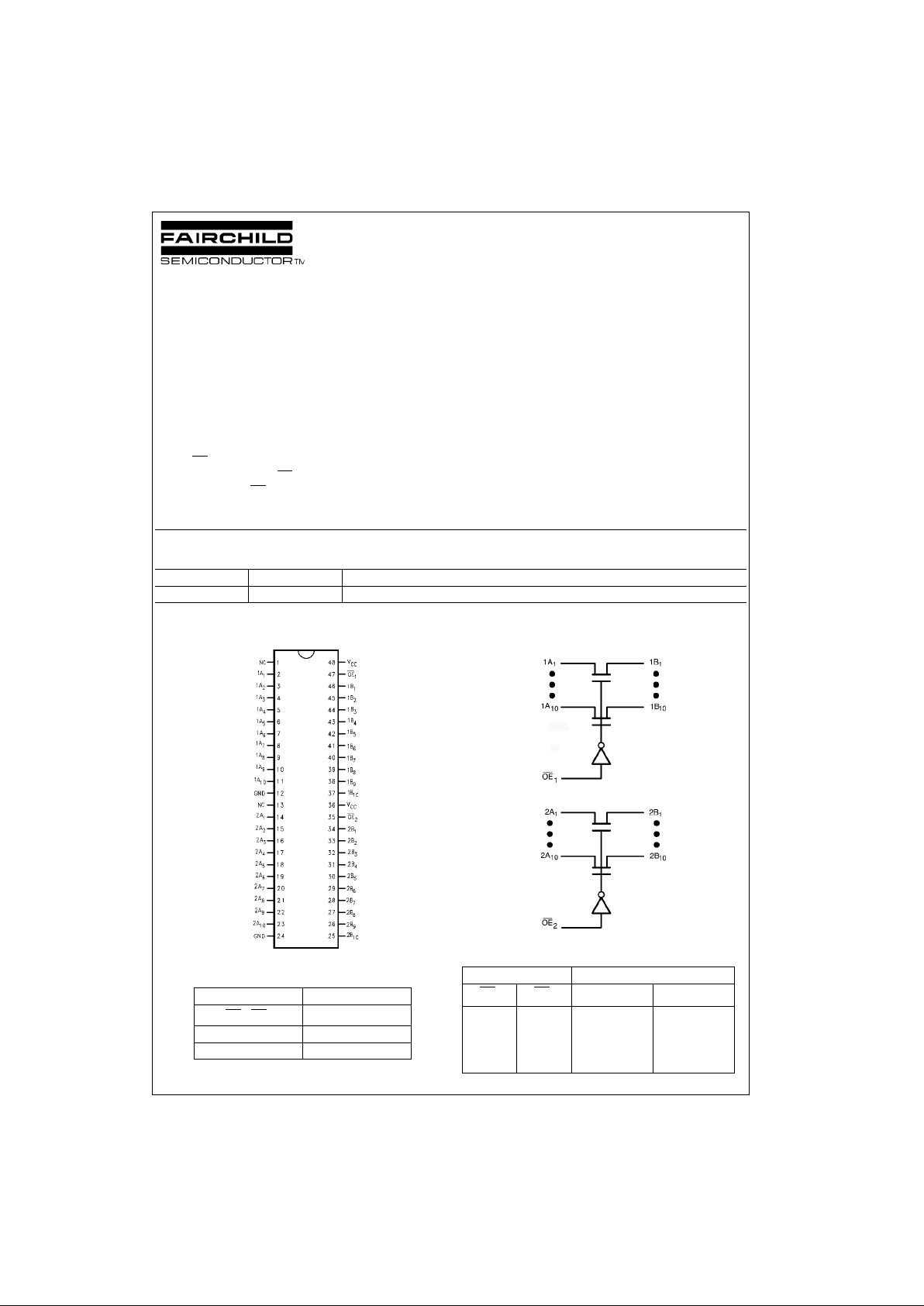
The device is organ ized as a 10-bit or 20-Bit bus switch.
When OE
1
is LOW, the switch is ON and Port 1A is con-
nected to Port 1B. When OE
2
is LOW, Port 2A is connected
to Port 2B. When OE
X
is HIGH, a high impedan ce state
exists between the A and B Ports.
Features
■ 4Ω switch connection between two ports.
■ Minimal propagation delay through the switch.
■ Low l
CC
.
■ Zero bounce in flow-through mode.
■ Control inputs compatible with TTL level.
Ordering Code:
Devices also availab le in Tape and Reel. Specify by appending th e s uffix let t er “X” to the ordering code.
Connection Diagram
Pin Descriptions
Logic Diagram
Truth T able
Order Number Package Number Package Description
FST16861MTD MTD48 48-Lead Thin Shrink Small Outline Package (TSSOP), JEDEC MO-153, 6.1mm Wide
Pin Name Description
OE
1
, OE
2
Bus Switch Enables
1A, 2A Bus A
1B, 2B Bus B
Inputs Inputs/Outputs
OE
1
OE
2
1A, 1B 2A, 2B
LL1A = 1B 2A = 2B
LH1A = 1B Z
HL Z 2A = 2B
HH Z Z
www.fairchildsemi.com 2
FST16861
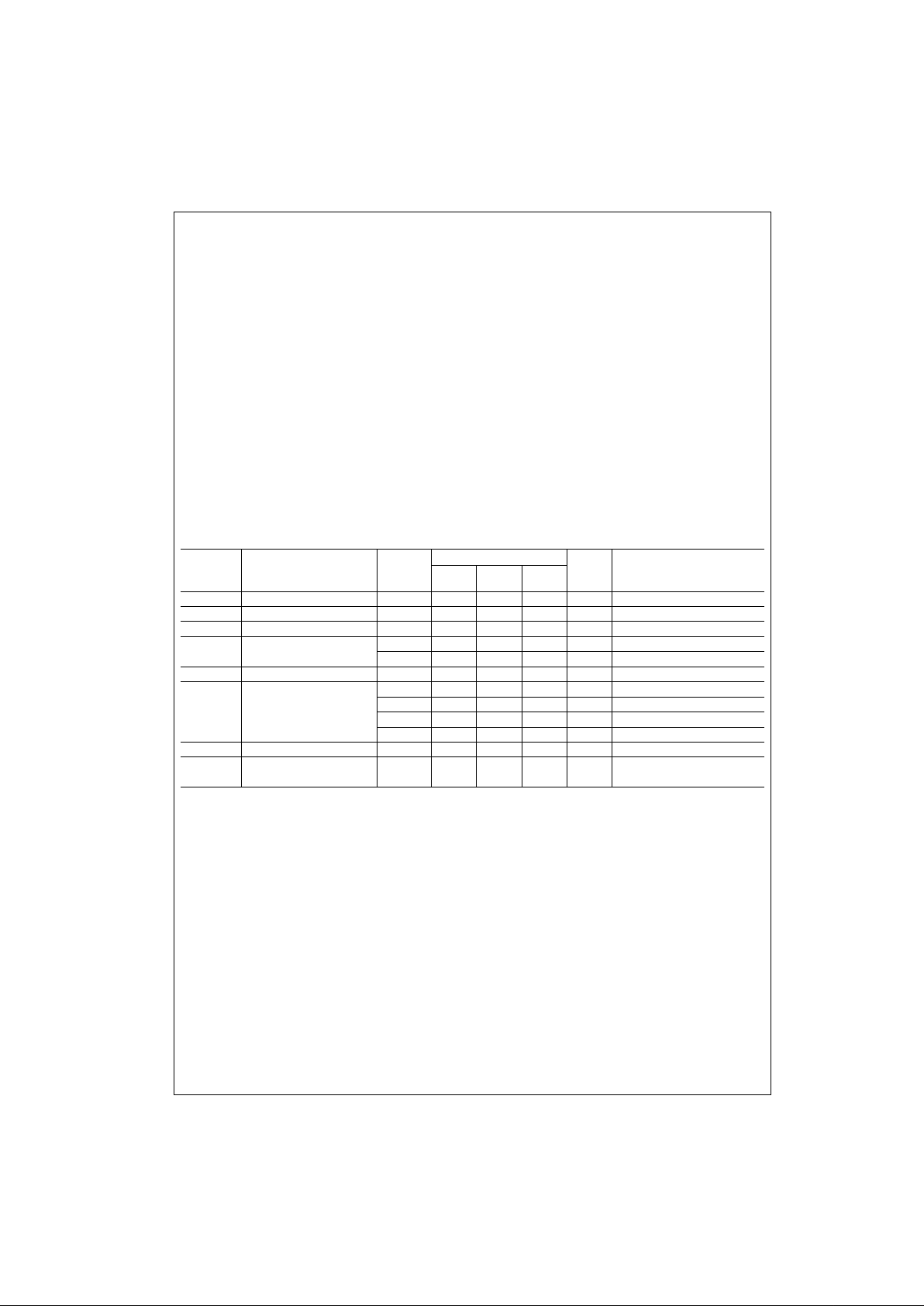
Absolute Maximum Ratings(Note 1) Recommended Operating
Conditions
(Note 4)
Note 1: The “Absolute Maximum Ratin gs” are those v alues beyon d which
the safety of the dev ice cannot be guaranteed. T he device sh ould not be
operated at these limits. The parametric values defined in the Electrical
Characteristics tables are not guaranteed at the absolute maximum rating.
The “Recommend ed O peratin g Cond itions” t able w ill defin e the co ndition s
for actual device operation.
Note 2: V
S
is the voltage observed/applied at either the A or B Ports across
the switch.
Note 3: The input and output negative volt age ratin gs may be exceede d if
the input and output diode current ratings are observed.
Note 4: Unused control inputs must be held high or low. They may not float.
DC Electrical Characteristics
Note 5: Typical values are at VCC = 5.0V and TA = +25°C
Note 6: Measured by th e v olt age drop between A and B pins at the indicated c urrent through the switc h. On resistance is det erm ined by the lower of the
voltages on the two (A or B) pins.
Supply Voltage (VCC)0.5V to +7.0V
DC Switch Voltage (V
S
) (Note 2) −0.5V to +7.0V
DC Input Voltage (V
IN
) (Note 3) −0.5V to +7.0V
DC Input Diode Current (l
IK
) VIN<0V −50mA
DC Output (I
OUT
) Current 128mA
DC V
CC
/GND Current (ICC/I
GND
) ±100mA
Storage Temperature Range (T
STG
) −65°C to +150 °C
Power Supply Operating (V
CC)
4.0V to 5.5V
Input Voltage (V
IN
)0V to 5.5V
Output Voltage (V
OUT
)0V to 5.5V
Input Rise and Fall Time (t
r
, tf)
Switch Control Input 0nS/V to 5nS/V
Switch I/O 0nS/V to DC
Free Air Operating Temperature (T
A
)-40 °C to +85 °C
Symbol Parameter
V
CC
(V)
TA = −40 °C to +85 °C
Units Conditions
Min
Typ
(Note 5)
Max
V
IK
Clamp Diode Voltage 4.5 −1.2 V IIN = −18mA
V
IH
HIGH Level Input Voltage 4.0–5.5 2.0 V
V
IL
LOW Level Input Voltage 4.0–5.5 0.8 V
I
I
Input Leakage Current 5.5 ±1.0 µA0 ≤ VIN ≤ 5.5V
0 ±1.0 µAVIN = 5.5V
I
OZ
OFF-STATE Leakage Current 5.5 ±1.0 µA0 ≤ A, B ≤ V
CC
R
ON
Switch On Resistance 4.5 4 7 Ω VIN = 0V, IIN = 64mA
(Note 6) 4.5 4 7 Ω VIN = 0V, IIN = 30mA
4.5 7 12 Ω VIN = 2.4V, IIN = 15mA
4.0 11 20 Ω VIN = 2.4V, IIN = 15mA
I
CC
Quiescent Supply Current 5.5 3 µAVIN = VCC or GND, I
OUT
= 0
∆ I
CC
Increase in I
CC
per Input 5.5 2.5 mA One input at 3.4V
Other inputs at VCC or GND
 Loading...