

Fairchild Semiconductor FJAF6808D Datasheet
FJAF6808D
High Voltage Color Display Horizontal
Deflection Output (Damper Diode Built In)
• High Collector-Base Breakdown Voltage : BV
• High Switching Speed : t
• For Color Monitor
(typ.) =0.1µs
F
CBO
= 1500V
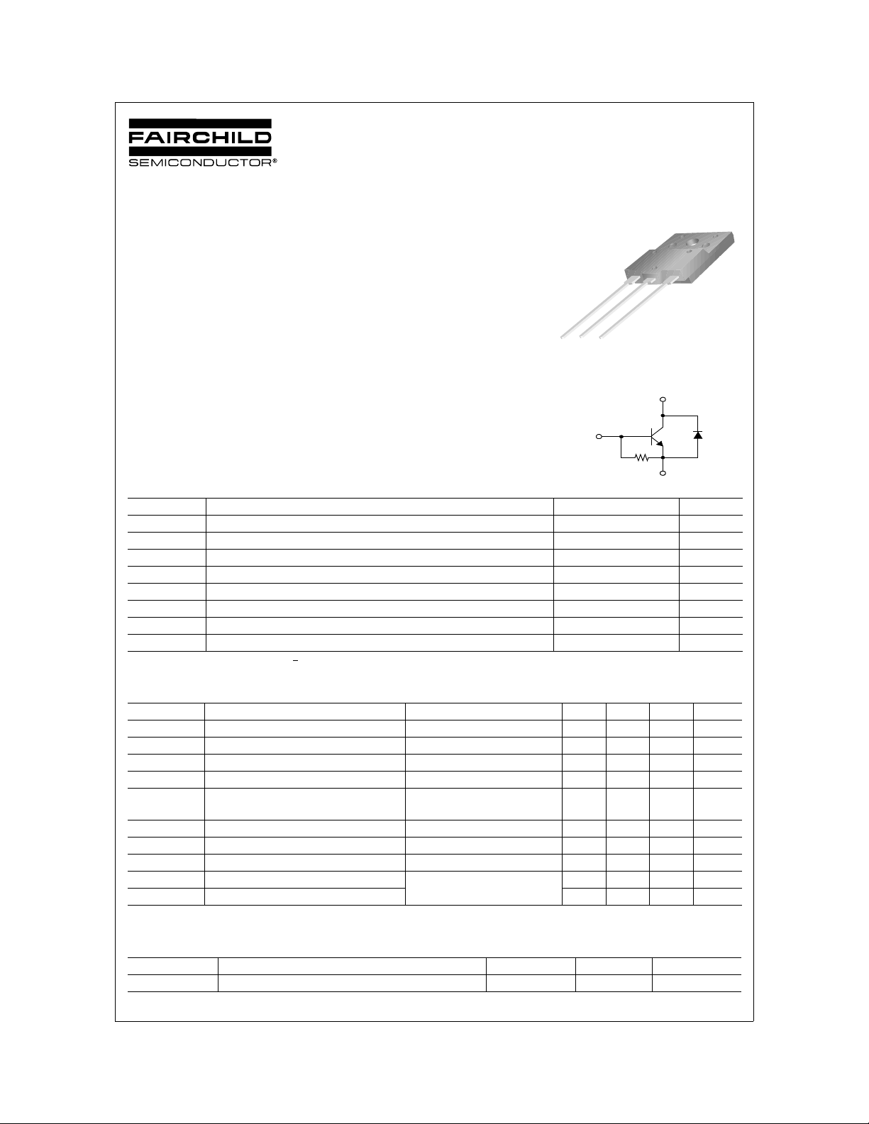
FJAF6808D
1
TO-3PF
1.Base 2.Collector 3.Emitter
Equivalent Circuit
C
B
NPN Triple Diffused Planar Silicon Transistor
Absolute Maximum Ratings
TC=25°C unless otherwise noted
45
Ω
typ.
E
Symbol Parameter Rating Units
V
CBO
V
CEO
V
EBO
I
C
* Collector Current (Pulse) 16 A
I
CP
P
C
T
J
T
STG
* Pulse Test: Pulse Width=5ms, Duty Cycle < 10%
Electrical Characteristics
Collector-Base Voltage 1500 V
Collector-Emitter Voltage 750 V
Emitter-Base Voltage 6 V
Collector Current (DC) 8 A
Collector Dissipation 50 W
Junction Temperature 150 °C
Storage Temperature - 55 ~ 150 °C
TC=25°C unless otherwise noted
Symbol Parameter Test Conditions Min. Typ. Max. Units
I
CES
I
CBO
I
EBO
BV
EBO
h
FE1
h
FE2
(sat) Collector-Emitter Saturation Voltage IC=5A, IB=1.2A 5 V
V
CE
(sat) Base-E mitter Saturat ion Voltage IC=5A, IB=1.2A 1.5 V
V
BE
V
F
* Storage Time VCC=200V, IC=4A, RL=50
t
STG
* Fall Time 0.2 µs
t
F
* Pulse Test: PW=20µs, duty Cycle=1% Pulsed
Collector Cut-off Current VCB=1400V, RBE=0 1 mA
Collector Cut-off Current VCB=800V, IE=0 10 µA
Emitter Cut-off Current VEB=4V, IC=0 40 200 mA
Base-Emitter Breakdown Voltage IE=300mA, IC=0 6 V
DC Current Gain VCE=5V, IC=1A
=5V, IC=5A
V
CE
7
4.5 7.5
Damper Diode Turn On Voltage IF = 4.5A 2 V
Ω
3 µs
IB1=1.0A, IB2= - 2.0A
Thermal Characteristics
TC=25°C unless otherwise noted
Symbol Parameter Typ. Max. Units
R
θjC
©2001 Fairchild Semiconductor Corporation Rev. A, October 2001
Thermal Resistance, Junction to Case 2.5 °C/W
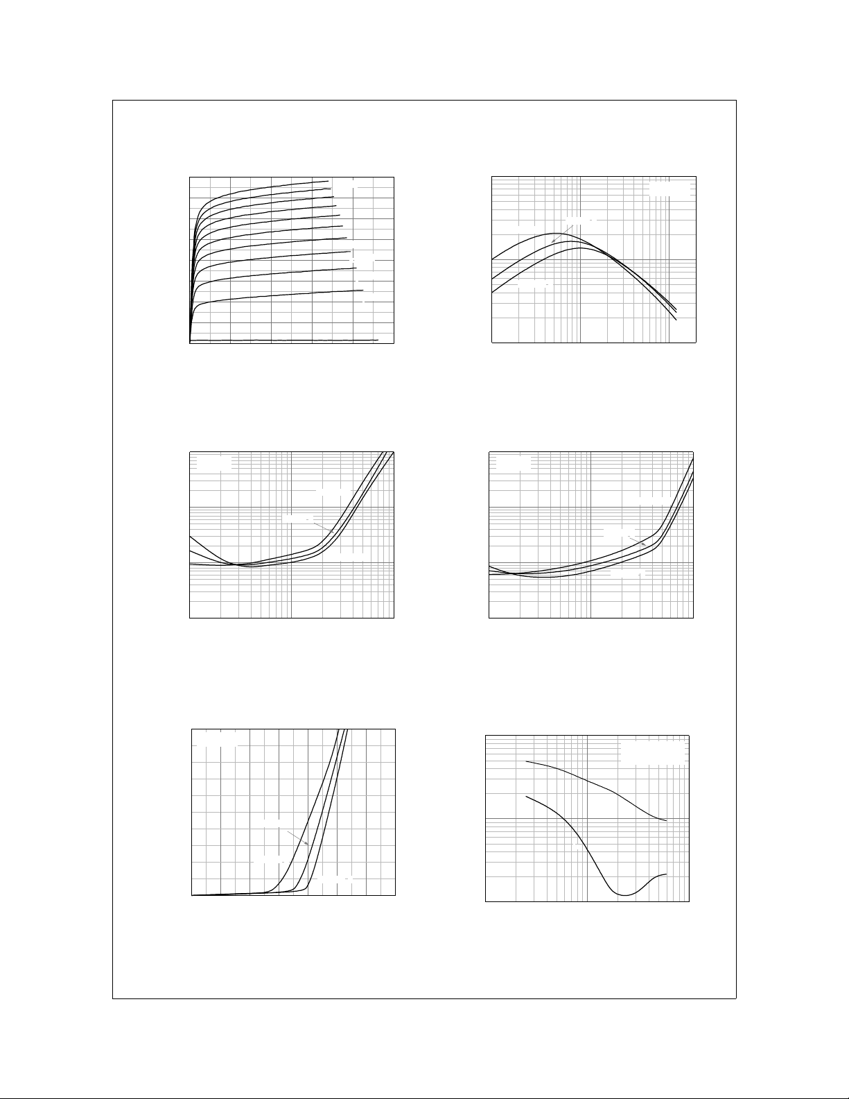
Typical Characteristics
FJAF6808D
8
7
6
5
4
3
2
[A], COLLECTOR CURRENT
C
I
1
0
0246810
IB = 2.0A
IB = 0.8A
IB = 0.6A
IB = 0.4A
IB = 0.2A
VCE [V], COLLECTOR-EMITTER VOLTAGE
100
Ta = 125 oC
10
, DC CURRENT GAIN
FE
h
Ta = - 25 oC
1
0.1 1 10
IC [A], COLLECTOR CURRENT
Figure 1. Static Characteristic Figure 2. DC current Gain
10
IC = 5 I
B
Ta = 125 oC
1
0.1
(sat) [V], SATURATION VOLTAGE
CE
V
0.01
0.1 1 10
Ta = 25 oC
Ta = - 25 oC
10
IC = 3 I
B
1
0.1
(sat) [V], SATURATION VOLTAGE
CE
V
0.01
0.1 1 10
VCE = 5 V
Ta = 25 oC
Ta = 125 oC
Ta = 25 oC
Ta = - 25 oC
Figure 3. Collector-Emitter Saturation Voltage Figure 4. Collector-Emitter Saturation Voltage
10
VCE = 5 V
8
6
4
2
[A], COLLECTOR CURRENT
C
I
0
0.0 0.2 0.4 0.6 0.8 1.0 1.2 1.4
VBE [V], BASE-EMITTER ON VOLTAGE
Figure 5. Base-Emitter On Voltage Figure 6. Resistive Load Switching Time
©2001 Fairchild Semiconductor Corporation
IC [A], COLLECTOR CURRENT
Ta = 25 oC
Ta = 125 oC
Ta = - 25 oC
IC [A], COLLECTOR CURRENT
10
1
s], SWITCHING TIME
µ
[
F
& t
STG
t
0.1
0.1 1 10
VCC = 200V,
I
t
STG
t
F
IB2 [A], REVERSE BASE CURRENT
= 4A, IB1 = 1A
C
Rev. A, October 2001
 Loading...