Fairchild Semiconductor FIN1108 Datasheet

FIN1108 • FIN1108T (Preliminary)
LVDS 8 Port High Speed Repeater
FIN1 108 • FIN1108T (Preliminary) LVDS 8 Port High Speed Repeater
March 2002
Revised May 2003
General Description
This 8 port repeater is designed for high speed interco nnects utilizing Low Voltage Differential Signaling (LVDS)
technology.
The FIN1108 accepts and outputs LVDS levels with a typi cal differential output swing of 330 mV w hich pro vides low
EMI at ultra low po wer dissipation even at hig h frequencies. The FIN1108 provides a V
pling on the inputs . In addition the FIN1108 can directly
accept LVPECL, HSTL, and SSTL-2 for translation to
LVDS.
The FIN1108T has internal termination across the receiver
inputs for reduced part count, reduced stub length and better noise immunity. See Applications section.
reference for AC co u-
BB
Features
■ Greater than 800 Mbps data rate
■ 3.3V power supply operation
■ 3.5 ps maximum random jitter and 135 ps maximum
deterministic jitter
■ Wide rail-to-rail common mode range
■ LVDS receiver inputs accept LVPECL, HSTL, and
SSTL-2 directly
■ Ultra low power consumption
■ 20 ps typical channel-to-chann el skew
■ Power off protection
■
> 7.5 kV HBM ESD Protection
■ Meets or exceeds the TIA/EIA-644-A LVDS standard
■ Available in space saving 48-lead TSSOP package
■ Open circuit fail safe protection
■ V
reference output
BB
■ FIN1108T (R
) features Internal Termination Resistors
T
Ordering Code:
Order Number Package Number Package Description
FIN1108MTD MTD48 48-Lead Thin Shrink Small Outline Package (TSSOP), JEDEC MO-153, 6.1mm Wide
FIN1108TMTD
(Preliminary)
Devices also availab l e in Tape and Reel. Specify by appending su ffix let te r “X” to the ordering code.
MTD48 48-Lead Thin Shrink Small Outline Package (TSSOP), JEDEC MO-153, 6.1mm Wide
© 2003 Fairchild Semiconductor Corporation DS500655 www.fairchildsemi.com

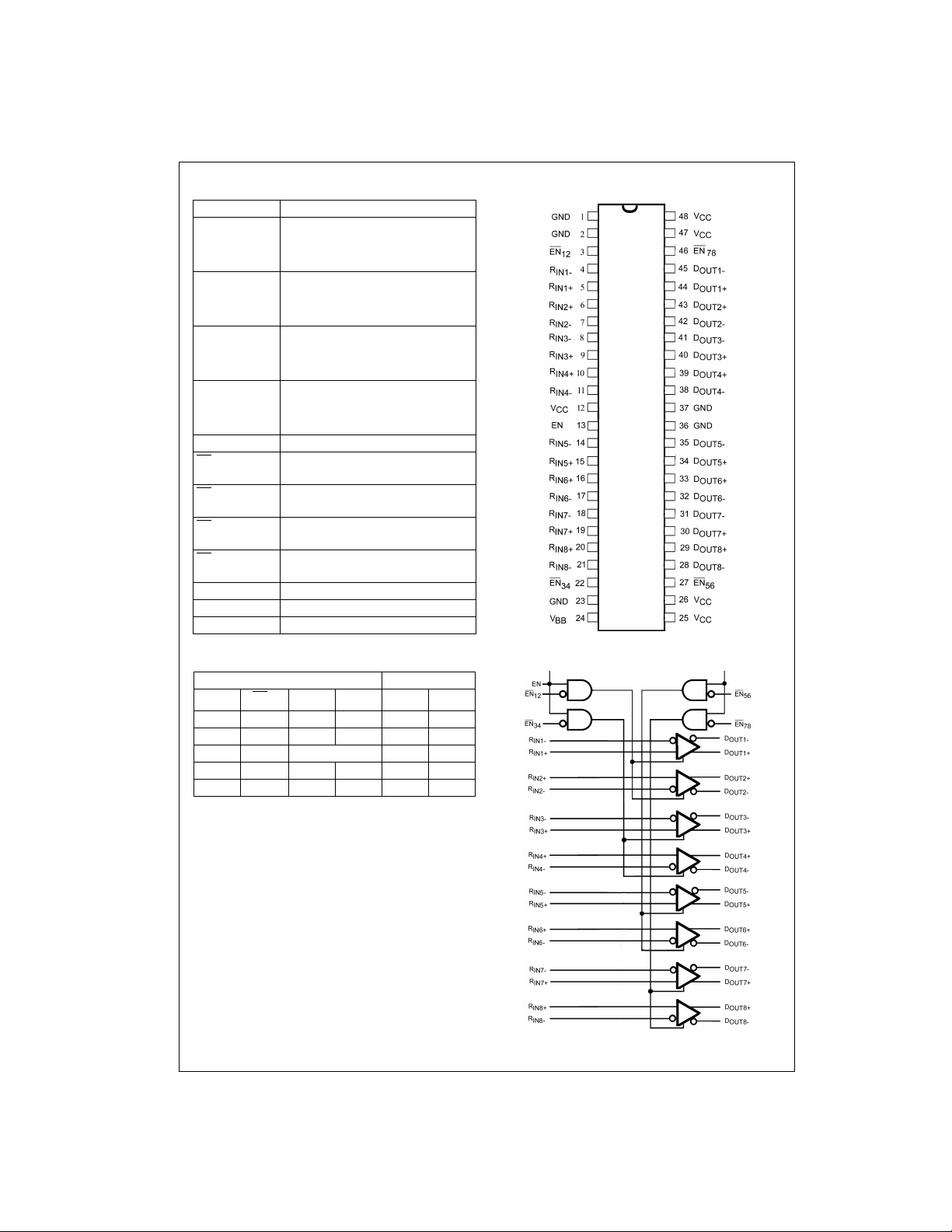
Pin Descriptions
Pin Name Description
R
, R
,
IN1+
IN2+
, R
R
IN3+
IN4+
R
, R
IN5+
IN6+
, R
R
IN7+
IN8+
R
, R
IN1−
IN2−
R
, R
IN3−
IN4−
, R
R
IN5−
IN6−
, R
R
IN7−
IN8−
D
, D
OUT1+
, D
D
OUT3+
, D
D
OUT5+
D
, D
OUT7+
D
, D
OUT1−
, D
D
OUT3−
D
, D
OUT5−
FIN1108 • FIN1108T (Preliminary)
D
OUT7−
, D
EN Driver Enable Pin for All Output
EN
12
EN
34
EN
56
EN
78
V
CC
GND Ground
V
BB
Non-inverting LVDS Input
,
,
,
Inverting LVDS Input
,
,
,
Non-inverting Driver Output
OUT2+
,
OUT4+
,
OUT6+
OUT8+
,
Inverting Driver Output
OUT2−
,
OUT4−
,
OUT6−
OUT8−
Inverting Driver Enable Pin for
and D
D
OUT1
Inverting Driver Enable Pin for
and D
D
OUT3
Inverting Driver Enable Pin for
and D
D
OUT5
Inverting Driver Enable Pin for
and D
D
OUT7
Power Supply
Reference Voltage Output
OUT2
OUT4
OUT6
OUT8
Connection Diagram
Function Table
Inputs Outputs
EN
EN
HL HLHL
HL LHLH
H L Fail Safe Case H L
XHXXZZ
LXXXZZ
H = HIGH Logic Level
L = LOW Logic Level
X = Don’t Care
Z = High Impedance
www.fairchildsemi.com 2
D
IN+
D
IN−DOUT+DOUT−
xx
Functional Diagram

Applications
Signal Optimization via Internal Termination
For LVDS signaling in point-to-point applications, receivers
or repeaters with on-chip termination are preferable to
reduce the overshoot or undersho ot due to the reflection
caused by stubs at receiver inputs. As a rule of thumb, usually the termination resistor for an LVDS receiver should be
placed as close as pos sible to the receiver, especially f or
high speed application s. If the distance between ter mination resistors and re ceivers i s too lon g, the in terc onnect ion
will be seen as an un-terminated stub which can produce
reflections resulting in h igher EM I. Inte rnal term ination c an
effectively smooth out this ringing which can otherwise
jeopardize the recei ver nois e margin. T his is impor tant for
Advantages: Disadvantages:
1. Reduced device count resulting in reduced board space
and production cost.
2. Reduced reflections caused by the stub length on the
receiver inputs, improving the signal integrity.
reliable high-speed operation with tighter required signal
settling times. Belo w is a list of the advan tages/disadvantages of internal termination.
Internal termination is not suitable for all ap plications. In
order to set a proper V
with on-chip termination resistors only work for point-topoint applications since multi-drop applications would
require terminatio n resistor for ea ch receiver, reducing the
equivalent termination to R
output swing by n.
1. Without special process treatment, on-chip termination can
experience greater temperature variation. This is usually
tolerable for low speed applications that have a sufficient
unit interval.
2. For applications with high common-mode noise, a center
tapped capacitor at the receiver side is desirable to filter
out the common-mode voltage noise of the input LVDS signal. This scheme works for an external termination scheme
with two (50
half-value termination resistors connected in series and
center tapped to a capacitor to Ground. To implement this
scheme using internal termina tion resistors, a center tap
pin would have to be used. This would increase the package size of the part.
at the driver outputs, receiv ers
OD
. This would re duc e t h e dr iv e r
T/n
Ω each for nominal 100Ω termination resistor)
FIN1108 • FIN1108T (Preliminary)
3 www.fairchildsemi.com
 Loading...