Fairchild Semiconductor FIN1104 Datasheet

FIN1104
LVDS 4 Port High Speed Repeater
FIN1 104 LVDS 4 Port High Speed Repeater
January 2002
Revised January 2003
General Description
This 4 port repeater is designed for high speed interco nnects utilizing Low Voltage Differential Signaling (LVDS)
technology. The FIN1104 accepts and outputs LVDS levels
with a typical differential output swing of 330 mV which provides low EMI at ultr a low power dissipation even at high
frequencies. The FIN1104 provides a V
coupling on the inputs. In add ition the F IN 1104 can directly
accept LVPECL, HSTL, and SSTL-2 for translation to
LVDS.
reference for AC
BB
Features
■ Greater than 800 Mbps data rate
■ 3.3V power supply operation
■ 3.5 ps maximum random jitter and 135 ps maximum
deterministic jitter
■ Wide rail-to-rail common mode range
■ LVDS receiver inputs accept LVPECL, HSTL, and
SSTL-2 directly
■ Ultra low power consumption
■ 20 ps typical channel-to-chann el skew
■ Power off protection
■
> 7.5 kV HBM ESD Protection
■ Meets or exceeds the TIA/EIA-644-A LVDS standard
■ Available in space saving 24-Lead TSSOP package
■ Open circuit fail safe protection
■ V
reference output
BB
Ordering Code:
Order Number Package Number Package Description
FIN1104MTC MTC24 24-Lead Thin Shrink Small Outline Package (TSSOP), JEDEC MO-153, 4.4mm Wide
Devices also availab l e in Tape and Reel. Specify by appending su ffix let te r “X” to the ordering code.
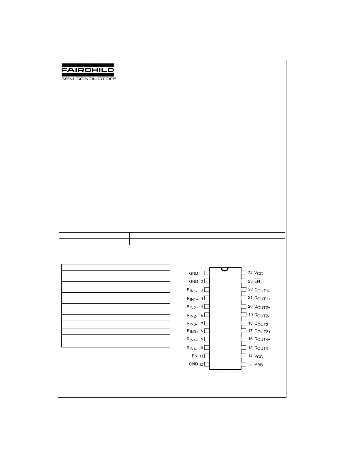
Pin Descriptions Connection Diagram
Pin Name Description
, R
,
R
IN1+
IN2+
, R
R
IN3+
IN4+
, R
R
IN1−
IN2−
, R
R
IN3−
IN4−
D
, D
OUT1+
, D
D
OUT3+
D
, D
OUT1−
, D
D
OUT3−
EN Driver Enable Pin for All Output
EN
V
CC
GND Ground
V
BB
Non-inverting LVDS Input
,
Inverting LVDS Input
,
Non-inverting Driver Output
OUT2+
OUT4+
,
Inverting Driver Output
OUT2−
OUT4−
Inverting Driver Enable Pin for all Outputs
Power Supply
Reference Voltage Output
© 2003 Fairchild Semiconductor Corporation DS500656 www.fairchildsemi.com

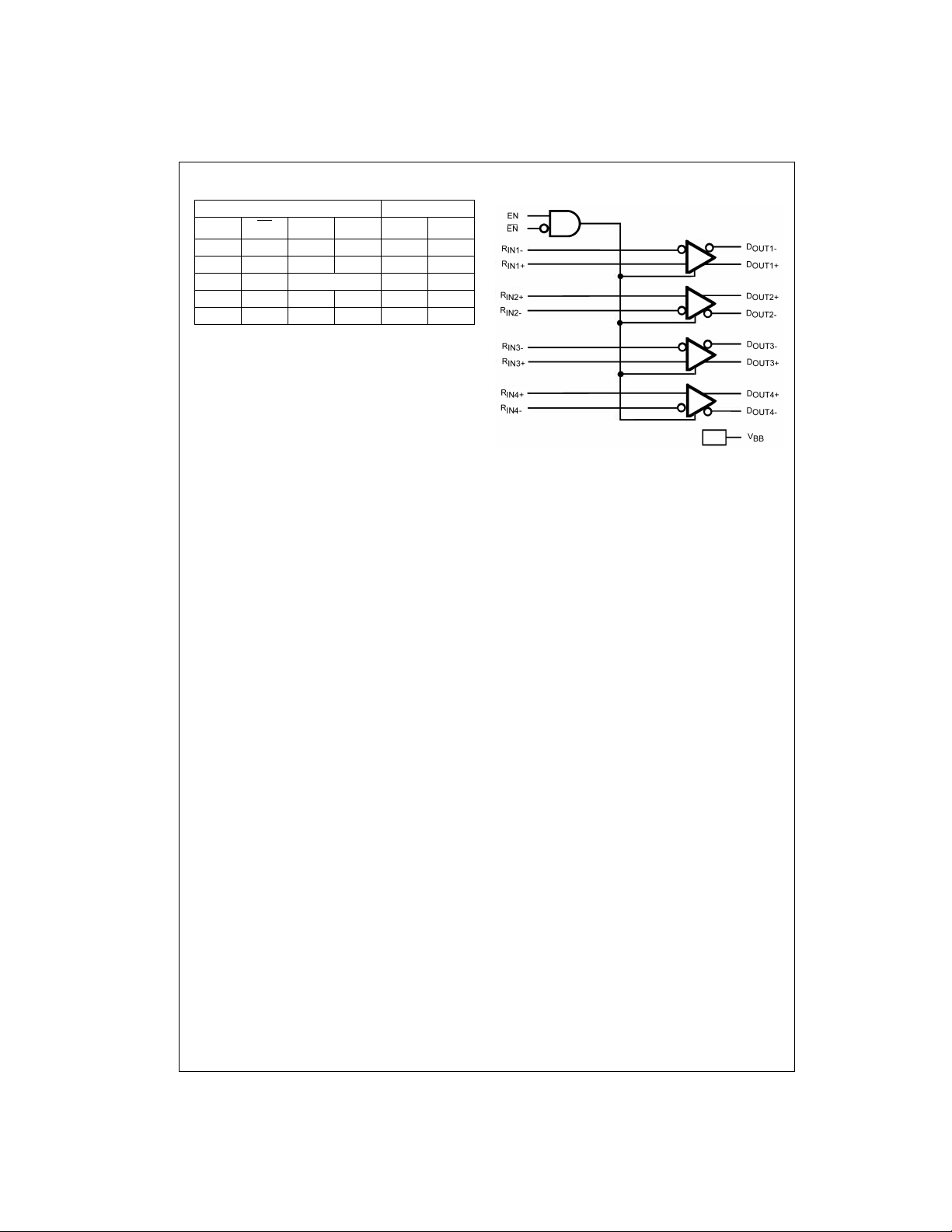
Function Table
Inputs Outputs
FIN1104
EN EN
HLHLHL
HLLHLH
H L Fail Safe Case H L
XHXXZZ
LXXXZZ
H = HIGH Logic Level
L = LOW Logic Level
X = Don’t Care
Z = High Impedance
D
D
IN+
IN−DOUT+DOUT−
Functional Diagram
www.fairchildsemi.com 2
 Loading...