

Fairchild Semiconductor FIN1102 Datasheet
FIN1102
LVDS 2 Port High Speed Repeater
FIN1 102 LVDS 2 Port High Speed Repeater
January 2002
Revised February 2002
General Description
This 2 port repeater is designed for high speed interco nnects utilizing Low Voltage Differential Signaling (LVDS)
technology. The FIN1102 accepts and outputs LVDS levels
with a typical differential output swing of 330 mV which provides low EMI at ultr a low power dissipation even at high
frequencies. The FIN1102 provides a V
coupling on the inputs. In addition the FIN1102 can also
directly accept LVPECL, HSTL, and SSTL-2 for translat ion
to LVDS.
reference for AC
BB
Features
■ Greater than 800 Mbps full differential path
■ 3.3V power supply operation
■ 3.5 ps maximum random jitter and 135 ps maximum
deterministic jitter
■ Wide rail-to-rail common mode range
■ LVDS receiver inputs accept LVPECL, HSTL, and
SSTL-2 directly
■ Ultra low power consumption
■ 20 ps typical channel-to-chann el skew
■ Power off protection
■
> 7 kV HBM ESD Protection
■ Meets or exceeds the TIA/EIA-644-A LVDS standard
■ 14-lead TSSOP package saves space
■ Open circuit fail safe protection
■ V
reference output
BB
Ordering Code:
Order Number Package Number Package Description
FIN1102MTC MTC14 14-Lead Thin Shrink Small Outline Package (TSSOP), JEDEC MO-153, 4.4mm Wide
Devices also availab l e in Tape and Reel. Specify by appending su ffix let te r “X” to the ordering code.
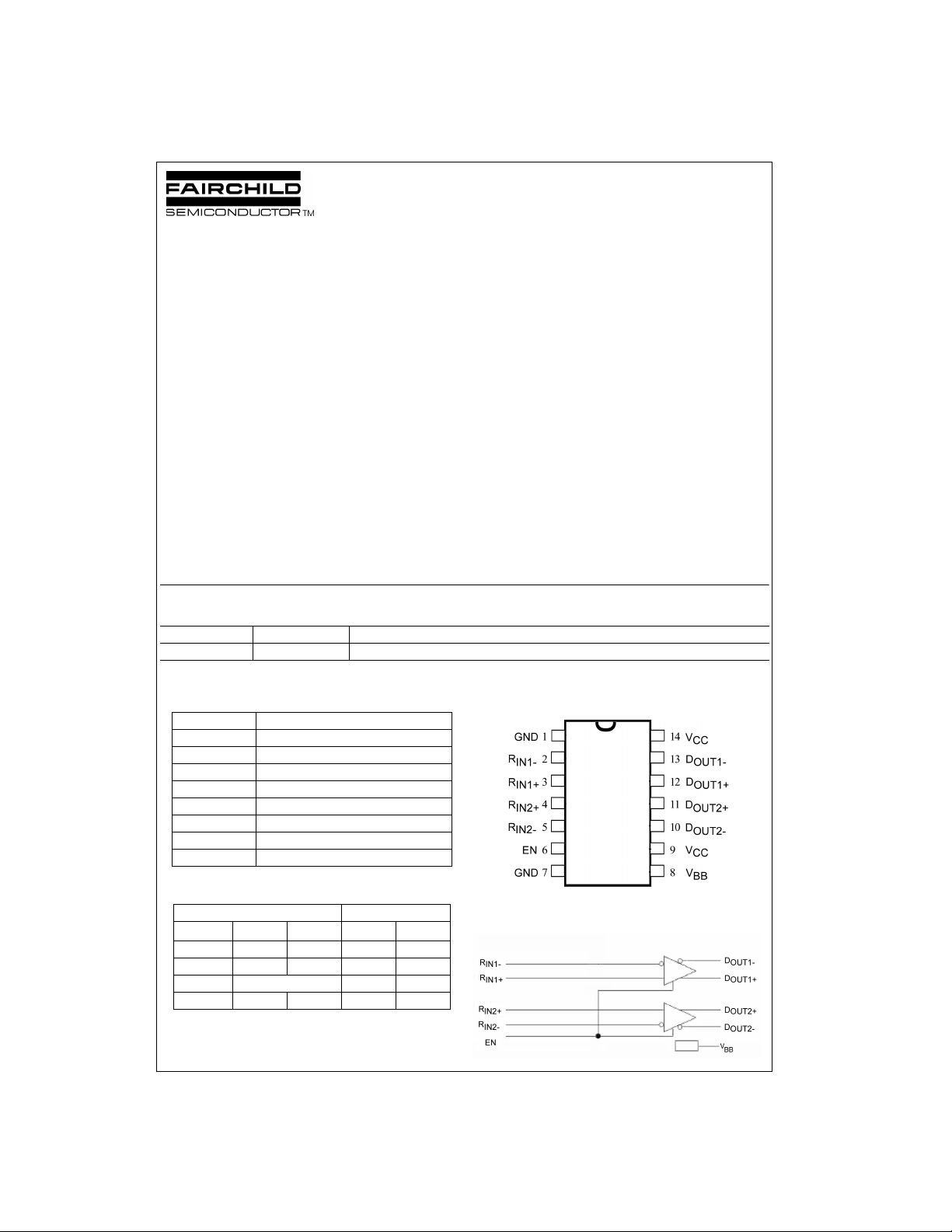
Pin Descriptions
Pin Name Description
, R
R
IN1+
R
, R
IN1−
D
, D
OUT1+
, D
D
OUT1−
EN Driver Enable Pin for All Output
V
CC
GND Ground
V
BB
Non-inverting LVDS Input
IN2+
Inverting LVDS Input
IN2−
Non-inverting Driver Output
OUT2+
Inverting Driver Output
OUT2−
Power Supply
Reference Voltage Output
Connection Diagram
Function Table
Inputs Outputs
EN
HHLHL
HLHLH
HFail Safe CaseH L
LXXZZ
H = HIGH Logic Le v el
L = LOW Logic Level
X = Don't Care
Z = High Impedance
© 2002 Fairchild Semiconductor Corporation DS500657 www.fairchildsemi.com
D
IN+
D
IN−
D
OUT+
D
OUT−
Functional Diagram
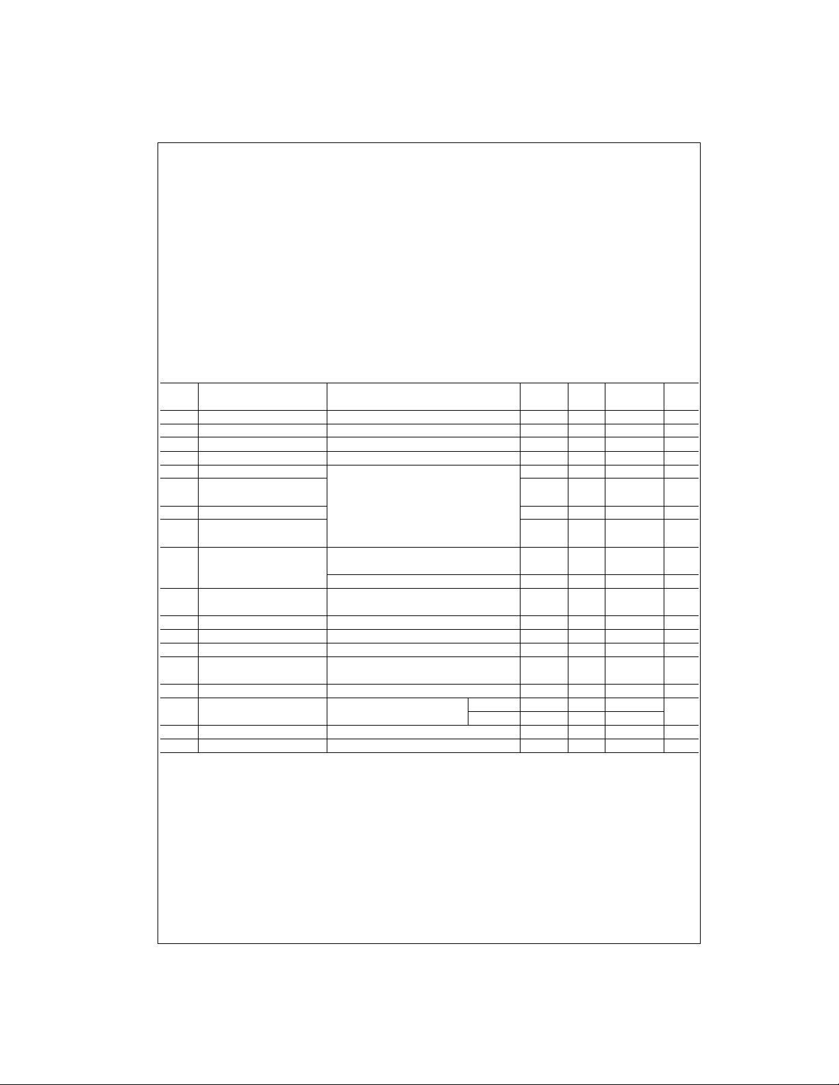
Absolute Maximum Ratings(Note 1) Recommended Operating
Supply Voltage (VCC) −0.5V to +4.6V
FIN1102
LVDS DC Input Voltage (V
LVDS DC Output Voltage (V
Driver Short Circuit Current (I
Storage Temperature Range (T
Max Junction Temperature (T
Lead Temperature (T
) −0.5V to +4.6V
IN
) −0.5V to +4.6V
OUT
) Continuous 10 mA
OSD
) −65°C to +150°C
STG
)150°C
J
)
L
(Soldering, 10 seconds) 260
ESD (Human B ody Model) 7000V
ESD (Machine Model) 300V
Conditions
Supply Voltage (V
Magnitude of Differential
Voltage (|V
Common Mode Voltage
Range (V
Operating Temperature (T
°C
Note 1: The “Absolute Maximum Ratings”: are those values beyond which
damage to the device may occur. The databook specifications should be
met, without exception, to ensure that the system design is reliable over its
power supply, temperatur e and output/input loading va riables. Fairchild
does not recommend operation of circu it s o ut s ide databook specific ation.
) 3.0V to 3.6V
CC
|) 100 mV to V
ID
)(0V + |VID|/2) to (VCC − |VID|/2)
IC
) −40°C to +85°C
A
DC Electrical Characteristics
Symbol Parameter Test Conditions
V
Differential Input Threshold HIGH See Figure 1; VIC = +0.05V, +1.2V, or VCC − 0.05V 100 mV
TH
V
Differential Input Threshold LOW See Figure 1; VIC = +0.05V, +1.2V, or VCC − 0.05V −100 mV
TL
V
Input HIGH Voltage (EN) 2.0 V
IH
V
Input LOW Voltage (EN) GND 0.8 V
IL
V
Output Differential Voltage 250 330 450 mV
OD
∆V
ODVOD
V
OS
∆V
OS
I
OS
I
IN
I
OFF
I
CCZ
I
CC
I
OZ
V
IC
C
IN
C
OUT
V
BB
Note 2: All typical values are at TA = 25°C and with VCC = 3.3V .
Magnitude Change from
Differential LOW-to-HIGH RL = 100 Ω, Driver Enabled,
Offset Voltage See Figure 2 1.125 1.23 1.375 V
Offset Magnitude Change from
Differential LOW-to-HIGH
Short Circuit Output Current D
Input Current (EN, D
Power Off Input or Output Current VCC = 0V, VIN or V
Disabled Power Supply Current Drivers Disabled 4 7 mA
Power Supply Current Drivers Enabled, Any Valid Input Con dition 16.7 23 mA
Disabled Output Leakage Current Driver Disabled, D
Common Mode Voltage Range |VID| = 100 mV to V
Input Capacitance Enable Input 2.5
Output Capacitance 2.8 pF
Output Reference Voltage VCC = 3.3V, IBB = 0 to −275 µA 1.125 1.2 1.375 V
INx+
, D
INx−
= 0V and D
OUT+
Driver Enabled
V
= 0V, Driver Enabled ±3.4 ±6mA
OD
)VIN = 0V to VCC, Other Input = VCC or 0V
(for Differential Inputs)
= 0V to 3.6V
D
OUT−
= 0V,
OUT−
= 0V to 3.6V ±20 µA
OUT
= 0V to 3.6V or
OUT+
CC
LVDS Input 2.1
Min Typ Max
(Note 2)
0V + |VID|/2 VCC − (|VID|/2) V
CC
Units
CC
25 mV
25 mV
−3.4 −6mA
±20 µA
±20 µA
V
pF
www.fairchildsemi.com 2
 Loading...