

Fairchild Semiconductor FIN1031 Datasheet
July 2001
Revised July 2001
FIN1031
3.3V LVDS 4-Bit High Speed Differential Driver
FIN1031 3.3V LVDS 4-Bit High Speed Differential Driver
General Description
This quad driver is designed for high speed inte rconnects
utilizing Low Voltage Differential Signaling (LVDS) technology. The driver translates LVTTL signal levels to LVDS levels with a typical differen tial output swin g of 350mV w hich
provides low EMI at ultra low power dissipation even at
high frequencies. Th is device is ideal for hi gh spe ed tran sfer of clock and data.
The FIN1031 can be paired with its companion receiver,
the FIN1032, or any other Fairchild LVDS receiver.
Features
■ Greater than 400Mbs data rate
■ 3.3V power supply operation
■ 0.4ns maximum differential pulse skew
■ 2.0ns maximum propagation delay
■ Low power dissipation
■ Power OFF protection
■ Meets or exceeds the TIA/EIA-644 LVDS standard
■ Pin compatible with equivalent RS-422 and LVPECL
devices
■ 16-Lead SOIC and TSSOP packages save space
Ordering Code:
Order Number Package Number Package Description
FIN1031M M16A 16-Lead Small Outline Integrated Circuit (SOIC), JEDEC MS-012, 0.150" Narrow
FIN1031MTC MTC16 16-Lead Thin Shrink Small Outline Package (TSSOP), JEDEC MO-153, 4.4mm Wide
Devices also availab le in Tape and Reel. Specify by appending the suffix letter “X” to the o rdering code.
Function Table
Inputs Outputs
EN EN
HXHHL
HXLLH
HXOPENLH
XLHHL
XLLLH
XLOPENLH
LHXZZ
H = HIGH Logic Le v el L = LOW Logic Level
X = Don’t Care Z = High Impedance
D
D
IN
OUT+
D
OUT−
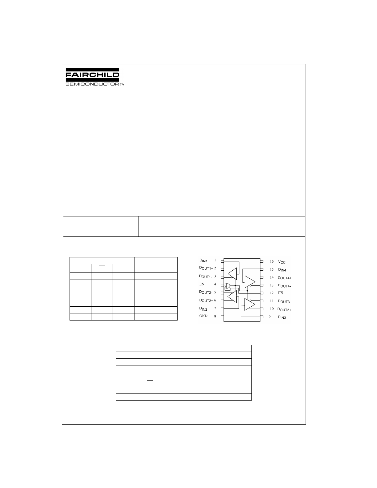
Connection Diagram
Pin Descriptions
Pin Name Description
, D
, D
D
IN1
D
, D
OUT1+
OUT1−
, D
OUT2+
OUT2−
D
© 2001 Fairchild Semiconductor Corporation DS500507 www.fairchildsemi.com
, D
IN2
IN3
IN4
, D
, D
OUT3+
, D
, D
OUT3−
EN Driver Enable Pin
EN
V
CC
GND Ground
LVTTL Data Inputs
Non-Inverting Driver Outputs
OUT4+
Inverting Driver Outputs
OUT4−
Inverting Driver Enable Pin
Power Supply
Absolute Maximum Ratings(Note 1) Recommended Operating
Supply Voltage (VCC) −0.5V to +4.6V
DC Input Voltage (V
FIN1031
@V
≥ 3V −0.5V to +6V
CC
= 0V −0.5V to +4.6V
@V
CC
DC Output Voltage (V
@V
= 0V −0.5V to +4.6V
CC
Driver Short Circuit Current (I
Storage Temperature Range (T
Max Junction Temperature (T
Lead Temperature (T
)
IN
)
OUT
) Continuous
OSD
) −65°C to +150°C
STG
) 150°C
J
)
L
(Soldering, 10 seconds) 260
ESD (Human Body Model)
ESD (Machine Model)
≥ 8000V
≥ 600V
Conditions
Supply Voltage (V
Input Voltage (V
Operating Temperature (TA) −40°C to +85°C
Note 1: The “Absolute Maximum Ratings”: are those values beyond which
damage to the device may occur. The databook specifications should be
°C
met, without exception, to ensure that the system design is reliable over its
power supply, temperatur e and output/input loading va riables. Fairchild
does not recommend operation of circu it s o ut s ide databook specific ation.
) 3.0V to 3.6V
CC
) 0 to V
IN
DC Electrical Characteristics
Over supply voltage and operating temperature ranges, unless otherwise specified
Symbol Parameter Test Conditions
V
OD
∆V
V
OS
∆V
I
OFF
I
OS
V
IH
V
IL
I
IN
I
OZ
I
I(OFF)
V
IK
I
CC
C
IN
C
OUT
Note 2: All typical values are at TA = 25°C and with VCC = 3.3V .
Output Differential Voltage 250 350 450 mV
VOD Magnitude Change from
OD
Differential LOW-to-HIGH RL = 100Ω, Driver Enabled,
Offset Voltage See Figure 1 1.125 1.25 1.375 V
Offset Magnitude Change from
OS
Differential LOW-to-HIGH
Power Off Output Current VCC = 0V, V
Short Circuit Output Current V
Input HIGH Voltage 2.0 V
Input LOW Voltage GND 0.8 V
Input Current VIN = 0V or V
Disabled Output Leakage Current EN = 0.8V, EN = 2.0V
Power-OFF Input Current VCC = 0V, VIN = 0V or 3.6V ±20 µA
Input Clamp Voltage IIK = −18 mA −1.5 V
Power Supply Current No Load, VIN = 0V or VCC, Driver Enabled 3.2 5
Input Capacitance 7pF
Output Capacitance 4pF
OUT
VOD = 0V, Driver Enabled ±6
V
OUT
= 100 Ω, Driver Disabled 3.2 5
L
RL = 100 Ω, VIN = 0V or VCC, Driver Enabled 17.9 25
= 0V or 3.6V ±20 µA
OUT
= 0V, Driver Enabled −6
CC
= 0V or 4.7V
Min Typ Max
(Note 2)
Units
25 mV
25 mV
mA
CC
±20 µA
±20 µA
mAR
CC
V
www.fairchildsemi.com 2
 Loading...