

Fairchild Semiconductor FIN1027 Datasheet
April 2001
Revised June 2003
FIN1027 • FIN1027A
3.3V LVDS 2-Bit High Speed Differential Driver
FIN1027 • FIN1027A 3.3V LVDS 2-Bit High Speed Differential Driver
General Description
This dual driver is design ed for high speed interconnects
utilizing Low Voltage Differential Signaling (LVDS) technology. The driver translates LVTTL signal levels to LVDS levels with a typical differen tial o utput swin g of 350 mV w hich
provides low EMI at ultra low power dissipation even at
high frequencies. Th is device is ideal for hi gh spe ed tran sfer of clock or data.
The FIN1027 or FI N1027A can be paired wi th its com panion receiver, the FIN1028, or with any other LVDS receiver.
Features
■ Greater than 600Mbs data rate
■ 3.3V power supply operation
■ 0.5ns maximum differential pulse skew
■ 1.5ns maximum propagation delay
■ Low power dissipation
■ Power-Off protection
■ Meets or exceeds the TIA/EIA-644 LVDS standard
■ Flow-through pinout simpli f ies PCB layout
■ 8-Lead SOIC, US8, and 8-terminal MLP
packages save space
Ordering Code:
Order Number Package Number Package Description
FIN1027M M08A 8-Lead Small Outline Integrated Circuit (SOIC), JEDEC MS-012, 0.150" Narrow
FIN1027MX M08A 8-Lead Small Outline Integrated Circuit (SOIC), JEDEC MS-012, 0.150" Narrow
FIN1027K8X MAB08A 8-Lead US8, JEDEC MO-187, Variation CA 3.1mm Wide
FIN1027MPX
(Preliminary)
FIN1027AM M08A 8-Lead Small Outline Integrated Circuit (SOIC), JEDEC MS-012, 0.150" Narrow
FIN1027AMX M08A 8-Lead Small Outline Integrated Circuit (SOIC), JEDEC MS-012, 0.150" Narrow
MLP08C 8-Terminal Molded Leadless Package (MLP) Dual, JEDEC MO-229, 2mm Square
[TUBE]
[TAPE and REEL]
[TAPE and REEL]
[TAPE and REEL]
[TUBE]
[TAPE and REEL]
© 2003 Fairchild Semiconductor Corporation DS500501 www.fairchildsemi.com
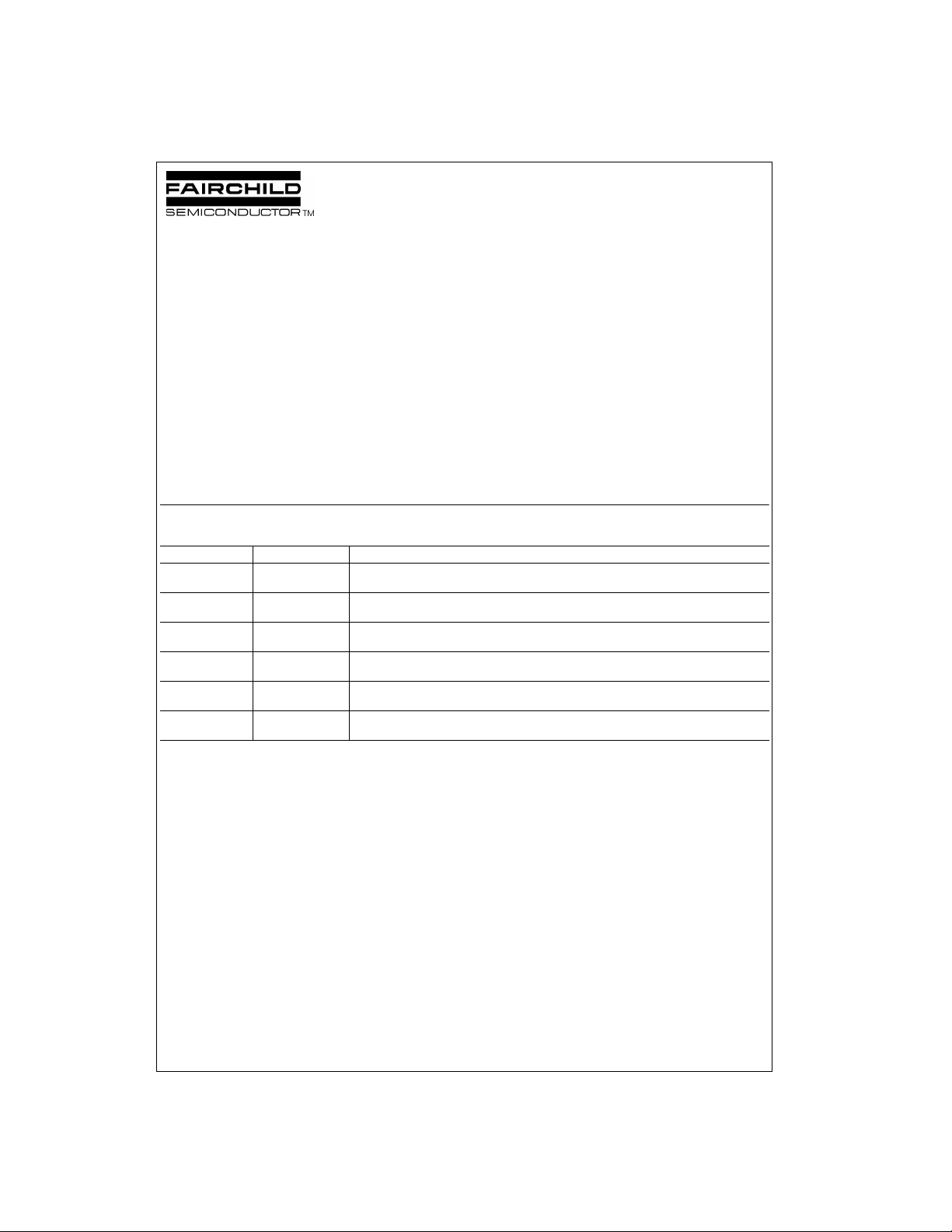
Connection Diagrams
FIN1027 • FIN1027A
Pin Assignments for SOIC
FIN1027
(Top View)
Pin Assignments for SOIC
FIN1027A
Pin Assignments f or US8
for FIN1027
(Top View)
Te rminal Assignments for M LP
FIN1027
(Top Through View)
(Top View)
Pin Descriptions Function Table
Pin Name Description
D
D
D
IN1
OUT1+
OUT1−
, D
IN2
, D
OUT2+
, D
OUT2−
V
CC
LVTTL Data Inputs
Non-inverting Driver Outputs
Inverting Driver Outputs
Power Supply
GND Ground
www.fairchildsemi.com 2
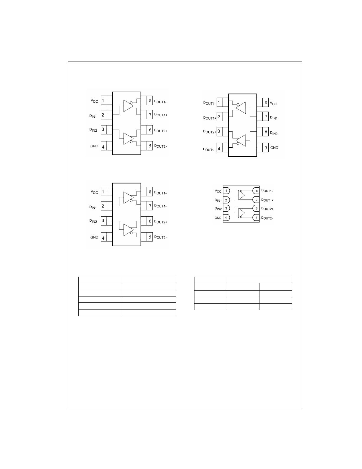
H = HIGH Logic Level
L = LOW Logic Level
X = Don’t Care
Input Outputs
D
IN
LLH
HHL
OPEN L H
D
OUT+
D
OUT−
Absolute Maximum Ratings(Note 1) Recommended Operating
Supply Voltage (VCC) −0.5V to +4.6V
DC Input Voltage (D
DC Output Voltage (D
Driver Short Circuit Current (I
Storage Temperature Range (T
Max Junction Temperature (T
Lead Temperature (T
) −0.5V to +6.0V
IN
) −0.5V to +4.7V
OUT
L
)
) Continuous
OSD
) −65°C to +150°C
STG
)150°C
J
(Soldering, 10 seconds) 260
ESD (Human Body Model)
ESD (Machine Model)
≥ 6500V
≥ 400V
Conditions
Supply Voltage (V
Input Voltage (V
Operating Temperature (TA) −40°C to +85°C
Note 1: The “Absolute Maximum Ratings”: are those valu es b eyo nd which
damage to the device may occur. The databook specifications should be
°C
met, without exception , to ensu re that the syst em design is reliab le over its
power supply, temperature and output/input loading variables. Fairchild
does not recommend operation of circuits outside databook specification.
) 3.0V to 3.6V
CC
) 0 to V
IN
DC Electrical Characteristics
Over supply voltage and operating temperature ranges, unless otherwise specified
Symbol Parameter Test Conditions
V
OD
∆V
V
OS
∆V
I
OFF
I
OS
V
IH
V
IL
I
IN
I
I(OFF)
V
IK
I
CC
C
IN
C
OUT
Note 2: All typical values are at TA = 25°C and with VCC = 3.3V.
Output Differential Voltage
VOD Magnitude Change from
OD
Differential LOW-to-HIGH
Offset Voltage 1.125 1.25 1.375 V
Offset Magnitude Change from
OS
Differential LOW-to-HIGH
Power Off Output Current VCC = 0V, V
Short Circuit Output Current V
Input HIGH Voltage 2.0 V
Input LOW Voltage GND 0.8 V
Input Current VIN = 0V or V
Power-Off Input Current VCC = 0V, VIN = 0V or 3.6V ±20 µA
Input Clamp Voltage IIK = −18 mA −1.5 V
Power Supply Current No Load, VIN = 0V or V
Input Capacitance 4pF
Output Capacitance 6pF
RL = 100 Ω, See Figure 1
= 0V or 3.6V ±20 µA
OUT
= 0V −8
OUT
VOD = 0V ±8
CC
R
= 100 Ω, VIN = 0V or V
L
CC
CC
Min Typ Max
(Note 2)
250 350 450 mV
Units
25 mV
25 mV
mA
CC
±20 µA
12.5 mA
17.0 mA
FIN1027 • FIN1027A
CC
V
3 www.fairchildsemi.com
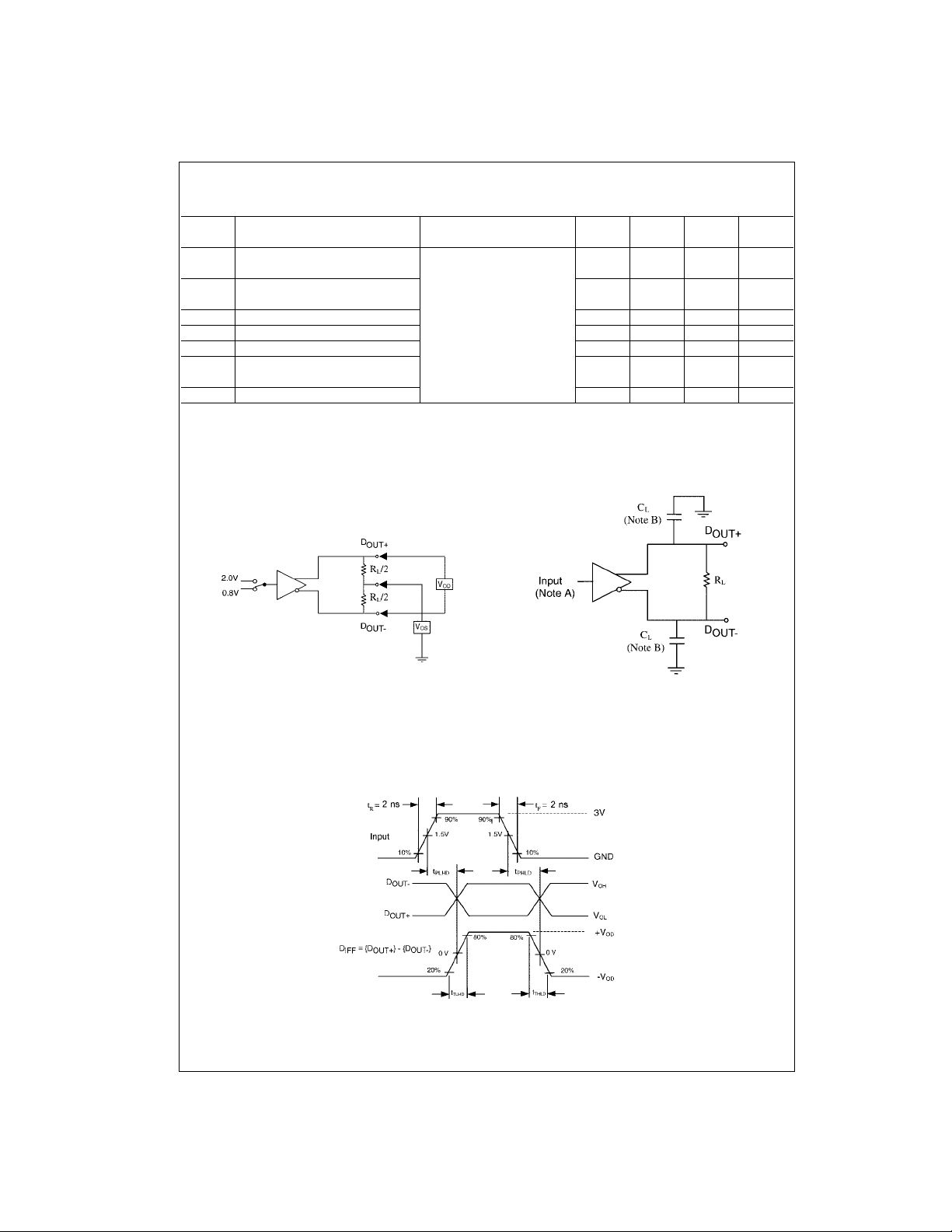
AC Electrical Characteristics
Over supply voltage and operating temperature ranges, unless otherwise specified
Symbol Parameter Test Conditions
t
PLHD
Differential Propagation Delay
LOW-to-HIGH
t
PHLD
Differential Propagation Delay
HIGH-to-LOW
t
FIN1027 • FIN1027A
TLHD
t
THLD
t
SK(P)
t
SK(LH)
t
SK(HL)
t
SK(PP)
Note 3: All typical values are at TA = 25°C and with VCC = 3.3V .
Note 4: t
tion.
Note 5: t
(either LOW-to-HI GH or HIGH-to-LOW) w hen both devices operate with the same supply voltage, same te m perature, and have id ent ic al test circuits.
Differential Output Rise Time (20% to 80%) RL = 100 Ω, CL = 10pF, 0.4 1.0 ns
Differential Output Fall Time (80% to 20%) See Figure 2 and Figure 3 0.4 1.0 ns
Pulse Skew |t
- t
| 0.5 ns
PLH
PHL
, Channel-to-Channel Skew
(Note 4)
Part-to-Part Skew (Note 5) 1.0 ns
, t
SK(LH)
SK(PP)
is the skew between speci fie d outputs of a s ingle device w hen the outputs have identical loads and are switching in t he same direc-
SK(HL)
is the magnitude of t he difference in propagation delay tim es between any spec ified terminals of t w o devices switching in the sam e di re c ti on
Min Typ Max
(Note 3)
0.5 1.5 ns
0.5 1.5 ns
Units
0.3 ns
FIGURE 1. Differential Driver DC Test Circuit
FIGURE 3. AC Waveforms
www.fairchildsemi.com 4
Note A: All input pulses have freq uency = 10 MHz, tR or tF = 2 ns
includes all probe and fixture capacitance s
Note B: C
L
FIGURE 2. Differential Driver Propagation Delay and
Transition Time Test Circuit
 Loading...