Fairchild Semiconductor FIN1022 Datasheet

FIN1022
2 X 2 LVDS High Speed Crosspoint Switch
FIN1022 2 X 2 L V DS High Speed Crosspoint Switch
September 2001
Revised December 2001
General Description
This non-blocking 2x 2 crosspoint switch has a fully differential input to output data path for low noise generation and
low pulse width distortion. The device can be used as a
high speed crosspoint sw itch, 2:1 multi plexer, 1:2 demultiplexer or 1:2 signal splitter. The inputs can directly interface
with LVDS and LVPECL levels.
Features
■ Low jitter, 800 Mbps full differential data path
■ Worst case jitter of 190ps
with PRBS
■ Rail-to-rail common mode range is 0.5V to 3.25V
■ Worst case power dissipation is less than 126 mW
■ Open-circuit fail safe protection
■ Fast switch time of 1.1 ns typical
■ 35 ps typical pin channel to channel skew
■ 3.3V power supply operation
■ Non-blocking switch
■ LVDS receiver inputs accept LVPECL signals directly
■ 7.5 kV HBM ESD protection
■ 16-lead SOIC package and TSSOP package
■ Inter-operates with TIA/EIA 644-1995 specification
■ See the Fairchild Inter face Sol ut ions we b page for cross
reference information:
www.fairchildsemi.com/products/interface/lvds.html
23
= 2
− 1 data pattern at 800 Mbps
Ordering Code:
Order Number Package Number Package Description
FIN1022M M16A 16-Lead Small Outline Integrated Circuit (SOIC), JEDEC MS-012, 0.150" Narrow
FIN1022MTC MTC16 16-Lead Thin Shrink Small Outline Package (TSSOP), JEDEC MO-153, 4.4mm Wide
Devices also availab l e in Tape and Reel. Specify by appending su ffix let te r “X” to the ordering code.
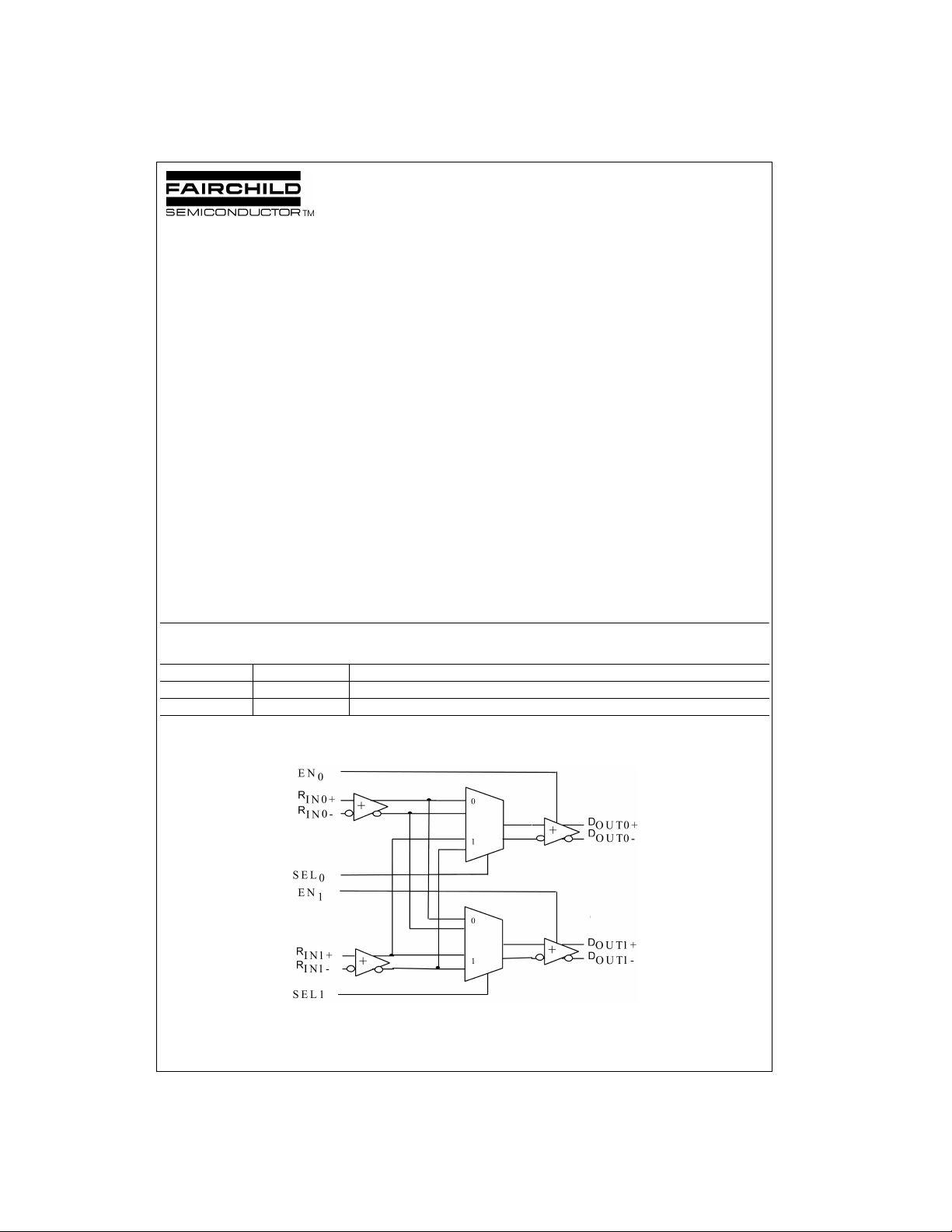
Logic Symbol
© 2001 Fairchild Semiconductor Corporation DS500653 www.fairchildsemi.com

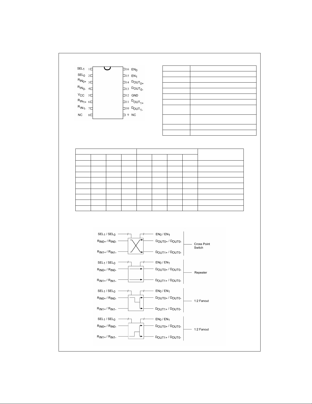
Connection Diagram Pin Descriptions
Pin Name Description
FIN1022
R
IN0+
R
IN0−
D
OUT0+
D
OUT0−
EN
EN
SEL
SEL
V
CC
, R
, R
, D
, D
0
1
0
1
LVDS non-inverting data inputs
IN1+
LVDS inverting data inputs
IN1−
LVDS non-inverting data outputs
OUT1+
LVDS inverting data outputs
OUT1−
LVTTL input for enabling D
LVTTL input for enabling D
LVTTL input for selecting R
R
IN1+/RIN1−
for output D
LVTTL input for selecting R
R
IN1+/RIN1−
for output D
Power Supply
GND Ground
Function Table
Inputs Outputs
SEL1EN
SEL
0
L / O L / O H H R
L / OHHHR
H L / O H H R
HHHHR
X L / O L / O H Z Z R
XHL / OHZZR
L / O X H L / O R
H X H L / O R
XXL / OL / OZZZZD
O = OPEN L / O = LOW or OPEN H = HIGH Logic Level L = LOW Logic Level X = Don’t Care Z = High Impedance
0
EN1D
OUT0+DOUT0−DOUT1+DOUT1−
IN0+RIN0−RIN0+RIN0−
IN0+RIN0−RIN1+RIN1−
IN1+RIN1−RIN0+RIN0−
IN1+RIN1−RIN1+RIN1−
IN0+RIN0−DOUT0
IN1+RIN1−DOUT0
IN0+RIN0−
IN1+RIN1−
ZZD
ZZD
1:2 Splitter
Repeater
Switch
1:2 Splitter
Disabled
Disabled
Disabled
OUT1
Disabled
OUT1
and D
OUT0
Mode
OUT1
OUT0+/DOUT0−
OUT1+/DOUT1−
IN0+/RIN0−
OUT0+/DOUT0−
IN0+/RIN0−
OUT1+/DOUT1−
Disabled
or
or
Function Diagrams
www.fairchildsemi.com 2

Absolute Maximum Ratings(Note 1) Recommended Operating
Supply Voltage (VCC) −0.3V to +4.6V
DC Input Voltage ( V
DC Output Voltage (V
Driver Short Circuit Current (I
Storage Temperature Range (T
Max Junction Temperature (T
Lead Temperature (T
) −0.3V to +4.6V
IN
) −0.3V to +4.6V
L
OUT
)
) Continuous
OSD
) −65°C to +150°C
STG
)150°C
J
(Soldering, 10 seconds) 260
Conditions
Supply Voltage (V
Input Voltage (V
Operating Temperature (TA) −40°C to +85°C
Electrostatic Discharge
(HBM 1.5 k
Electrostatic Discharge
°C
(MM 0Ω, 100 pF) >300V
Note 1: The “Absolute Maximum Ratings”: are those valu es b eyo nd which
damage to the device may occur. The databook specifications should be
met, without exception , to ensu re that the syst em design is reliab le over its
power supply, temperature and output/input loading variables. Fairchild
does not recommend operation of circuits outside databook specification.
) 3.0V to 3.6V
CC
) 0 to V
IN
Ω, 100 pF) >7500V
DC Electrical Characteristics
Over supply voltage and operating temperature ranges, unless otherwise specified (Note 2)
Symbol Parameter Test Conditions
LVDS Differential Driver Characteristics
V
OD
∆V
V
OS
∆V
I
OZD
I
OFF
I
OS
LVDS Differential Receiver Characteristics
V
TH
V
TL
V
IC
I
IND
LVTTL Control Characteristics
V
IH
V
IL
I
IN
Device Characteristics
V
IK
I
PU/PD
C
IN
C
OUT
I
CC
Note 2: This part will only function with datasheet specif ic at ion when a resistive load is applied to the driver outputs.
Note 3: All typical values are at T
Output Differential Voltage RL = 75 Ω, See Figure 3 270 365 475
TA = 25°C and VCC = 3.3V
VOD Magnitude Change from
OD
Differential LOW-to-HIGH
Offset Voltage See Figure 3 1.0 1.2 1.45 V
Offset Magnitude Change from
OS
Differential LOW-to-HIGH
Disabled Output Leakage Current V
Power-Off Current VCC = 0V, VIN or V
Short Circuit Output Current V
Differential Input Threshold HIGH VIC = 0.05V or 1.2V or 3.25V 100
Differential Input Threshold LOW VCC = 3.3V −100
Input Common Mode Voltage 0.05 3.25 V
Input Current (Differential Inputs) VIN = GND ±20
Input High Voltage 2 V
Input Low Voltage 0.8 V
Input Current VIN = 3.6V or GND ±20 µA
Input Clamp Voltage IIK = −18 mA −1.5 V
Output Power-Up/Power-Down
High Z Leakage Current
Input Capacitance 4.5 pF
Output Capacitance 4.5 pF
Power Supply Current No Load, All Drivers Enabled 35 mA
= 25°C and with VCC = 3.3V.
A
RL = 75 Ω, See Figure 3 35 mV
See Figure 3 35 mV
= 3.6V or GND, Driver Disabled ±10 µA
OUT
= 0V, Driver Enabled −10
OUT
V
= 0V, V
OUTx+
VIN = V
CC
VCC = 0V to 1.5V ±10 µA
RL = 75 Ω, All Drivers Enabled 35 mA
RL = 75 Ω, All Drivers Enabled 35 mA
= 3.6V or 0V ±20 µA
OUT
= 0V, Driver Enabled −10
OUTx−
Min Typ Max
(Note 3)
285 365 440
±20
FIN1022
CC
Units
mVRL = 75 Ω, See Figure 3
mA
mV
µA
3 www.fairchildsemi.com
 Loading...