

Fairchild Semiconductor FFPF06U150S Datasheet
Features
• High v ol tage and high rel ia bility
• High speed switching
• Low forward voltage
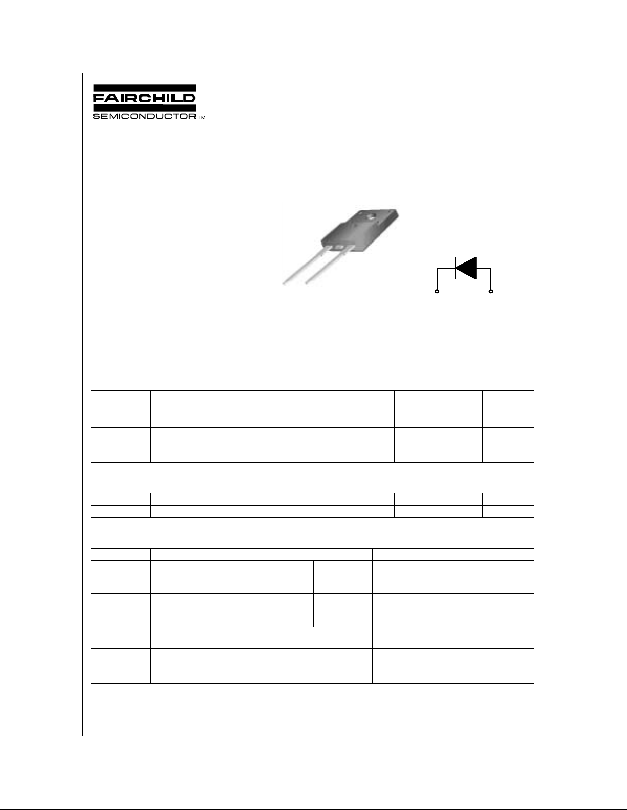
FFPF06U150S
FFPF06U150S
Applications
• Suitable for damper diode in horizontal
deflec tion circ ui t s
1 2
TO-220F
1. Cathode 2. Anode
DAMPER DIODE
Absolute Maximum Ratings
Symbol Parameter Value Units
V
RRM
I
F(AV)
I
FSM
T
J, TSTG
Peak Repetitiv e Reverse Volt age 1500 V
Average Rectified Forward Current @ TC = 125°C6 A
Non-repetitive Peak Surge Current
60Hz Single Ha lf- Sine Wave
Operating Junction and Storage Temperature - 65 to +150 °C
Thermal Characteristics
Symbol Parameter Value Units
R
θJC
Maxi mum Therm al Resist ance, Junction to Case 3.0 °C/W
Electrical C haract eri stics
Symbol Parameter Min. Typ. Max. Units
V
FM
*
I
RM
*
t
rr
t
fr
V
FRM
* Pulse Test: Pulse Width=300µs, Duty Cycle=2%
Maximum Instantaneous Forward Voltage
I
I
Maximum Instantaneous Reverse Current
@ rated V
Maximum Reverse Recovery Time
(I
=1A, di/dt = 50A/µs)
F
Maximum Forward Recovery Time
(I
=6.5A, di/dt = 50A/µs)
F
Maximum Forward Recovery Voltage - - 16 V
TC=25°°°°C unless otherwise noted
TC=25 °°°°C unless otherwise noted
= 6A
F
= 6A
F
TC = 25 °C
R
= 25 °C
T
C
T
= 125 °C
C
T
= 125 °C
C
60 A
-
-
-
-
--150ns
--350ns
-
-
-
-
1.8
1.7
10
80
V
µA
©2000 Fai r ch i ld Semiconductor Inter national
Rev. F, September 2000
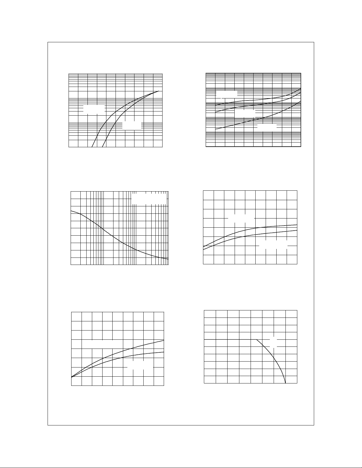
Typical C h aracteristic sTypical C h aracteristic s
FFPF06U150S
100
[A]
F
10
TJ = 125oC
1
Forward Current , I
0.1
0.0 0.4 0.8 1.2 1.6 2.0
TJ = 25oC
Forward Voltage , VF [V]
Figure 1. Typical Forward Voltage Drop
vs. Forward Current
200
180
160
140
120
100
80
60
Capacitance , Cj [pF]
40
20
0
0.1 1 10 100
Reverse Voltage , VR [V]
Typical Capacitanc e
at 0V = 150 pF
100
10
A]
µ
[
R
0.1
0.01
Reverse Current , I
0.001
TJ = 125oC
1
TJ = 100oC
TJ = 25oC
0 300 600 900 1200 1500
Reverse Voltage , VR [V]
Figure 2. Typical Reverse Current
vs. Revers e Voltag e
400
[ns]
rr
300
di/dt = 50A/µs
200
100
di/dt = 100A/µs
Reverse Recovery Time , t
0
12345678910
Forward Current , IF [A]
Figure 3. Typical Junction Capacitance
Figure 4. Typical Reverse Recovery Time
vs. Forward Current
2000
[nC]
rr
1500
1000
500
di/dt = 100A/µs
di/dt = 50A/µs
Stored Recovery Charge , Q
0
12345678910
Forward Current , IF [A]
Figure 5. Typical Stored Charge
10
[A]
9
F(AV)
8
7
6
5
4
3
2
1
Average Forward Current , I
0
80 100 120 140 160
DC
Case Temperature , TC [oC]
Figure 6. Forward Current Derating Curve
vs. Forward Current
©2000 Fai r ch i ld Semiconductor Inter national Rev. F, September 2000
 Loading...