

Fairchild Semiconductor FDZ2551N Datasheet
ADVANCE INFORMATION
1Q2
FDZ2551N
Dual N-Channel 2.5V Specified PowerTrenchTM BGA MOSFET
FDZ2551N
November 1999
General Description
Combining Fairchild’s advanced 2.5V specified
PowerTrench process with state of the art BGA
packaging, the FDZ2551N minim izes both PCB space
and R
. This dual BGA MOSFET embodies a
DS(ON)
breakthrough in packaging technology which enables
the device to combine excellent thermal transfer
characteristics, high current handling capability, ultralow profile packaging, low gate charge, and low R
DS(ON)
.
Applications
•= Battery management
•= Load switch
•= Battery protection
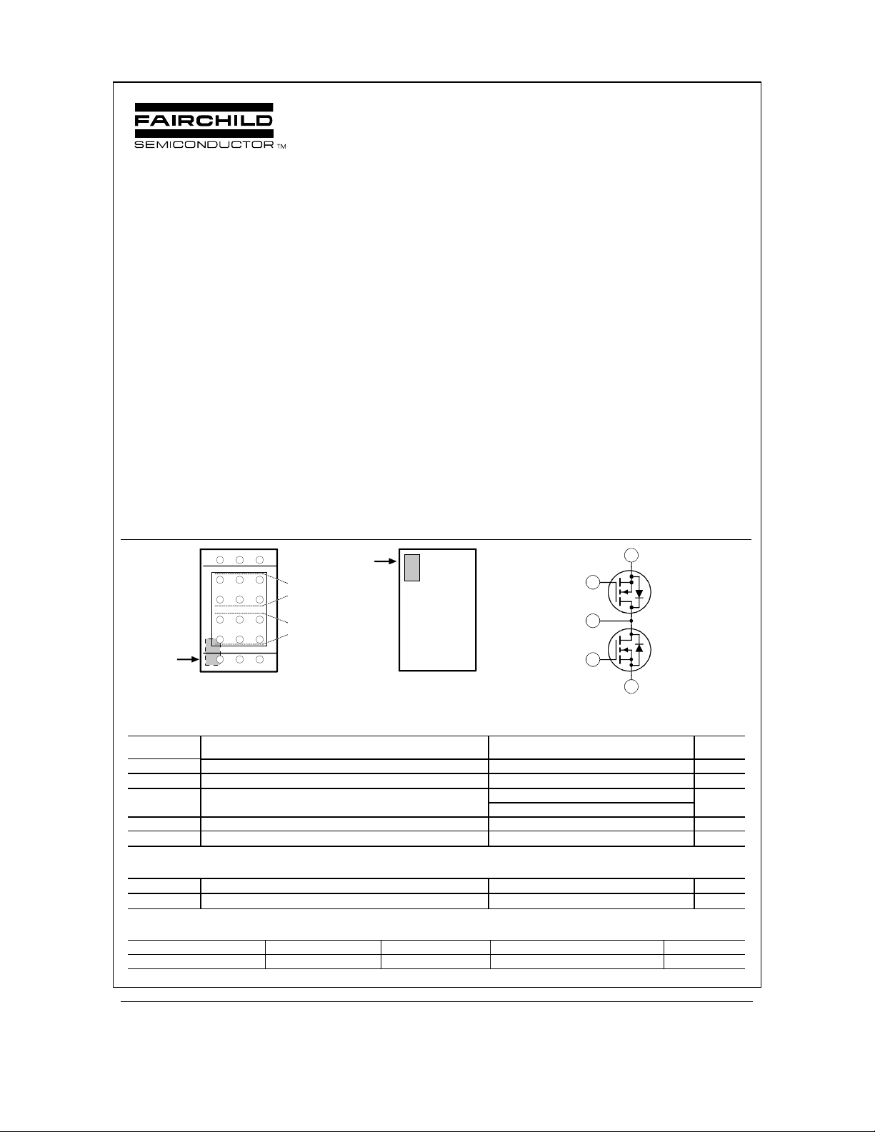
D D
Pin 1
S
S
S
G
S
S
G
S S
D D D
D
S
Q2
S
S
Q1
Pin 1
Bottom
Top
Features
•= 9 A, 20 V. R
R
•= Occupies only 0.10 cm
1/3 the area of SO-8.
•= Ultra-thin package: less than 0.70 mm height when
mounted to PCB.
•= Outstanding thermal t ransfer characteristic s:
significantly better than SO-8.
•= Ultra-low Q
x R
g
•= High power and current handling capability.
F2551
= 0.018 Ω=@ VGS = 4.5 V
DS(ON)
= 0.030 Ω @ VGS = 2.5 V.
DS(ON)
2
of PCB area.
figure-of-merit.
DS(ON)
S
G
D
G
S
Q
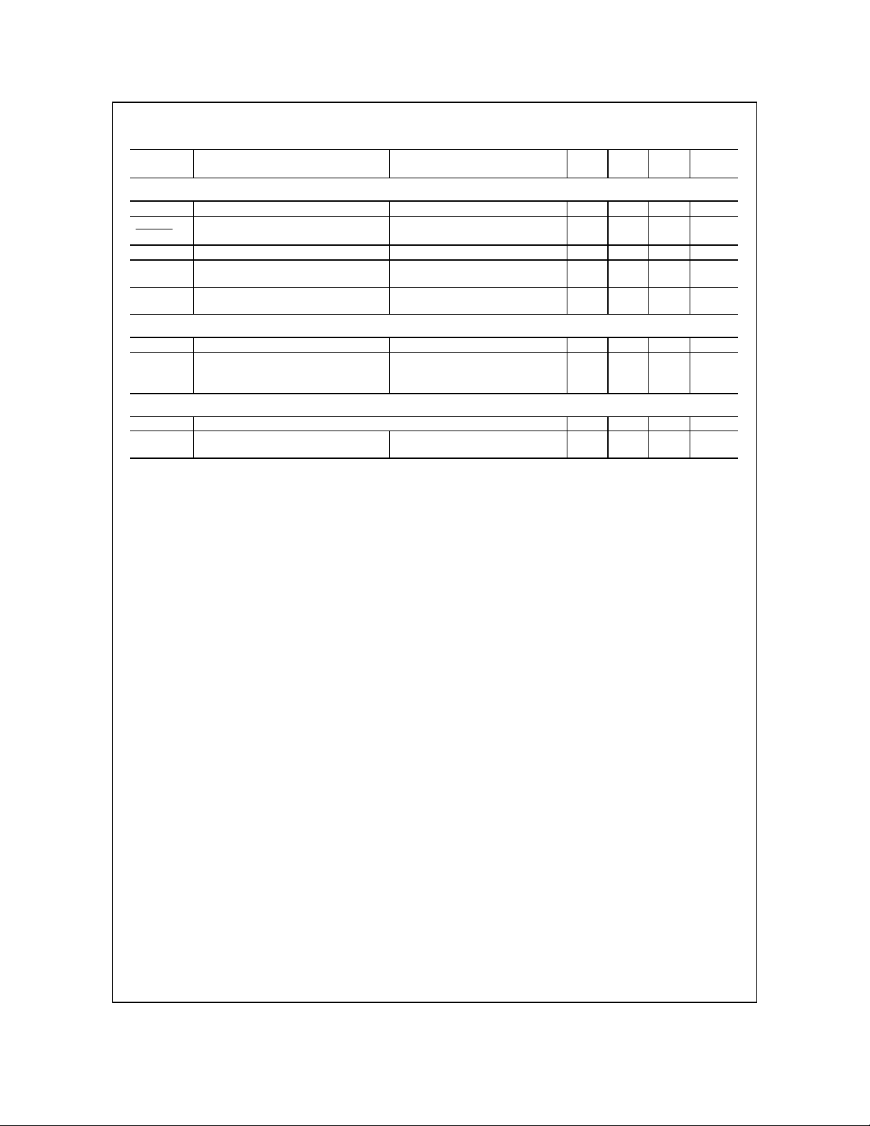
Absolute Maximum Ratings T
o
=25
C unless otherwise noted
A
Symbol Parameter Ratings Units
V
Drain-Source Voltage 20 V
DSS
V
Gate-Source Voltage
GSS
±12
V
ID Drain Current – Continuous (Note 1a) 9 A
– Pulsed 20
PD Power Dissipation (Steady State) (Note 1a) 3 W
TJ, T
Operating and Storage Junction Temperature Range -55 to +175
stg
°C
Thermal Characteristics
R
θJA
R
θJC
Thermal Resistance, Junction-to-Ambient
Thermal Resistance, Junction-to-Case
(Note 1a) 50
(Note 1) 8
°C/W
°C/W
Package Marking and Ordering Information
Device Marking Device Reel Size Tape width Quantity
F2551 FDZ2551N TBD TBD TBD
1999 Fairchild Semiconductor Corporation
FDZ2551N Rev A1(W)
FDZ2551N
Electrical Characteristics T
= 25°C unless otherwise noted
A
Symbol Parameter Test Conditions Min Typ Max Units
Off Characteristics
BV
Drain–Source Breakdown Voltage
DSS
∆BVDSS
===∆T
I
Zero Gate Voltage Drain Current VDS = 16 V, VGS = 0 V 1
DSS
I
GSSF
Breakdown Voltage Temperature
Coefficient
J
Gate–Body Leakage Current,
V
= 0 V, ID = 250 µA
GS
I
= 250 µA,Referenced to 25°C
D
VGS = 12 V, VDS = 0 V 100 nA
20 V
14
mV/°C
Forward
I
Gate–Body Leakage Current,
GSSR
VGS = –12 V VDS = 0 V –100 nA
Reverse
On Characteristics (Note 2)
V
Gate Threshold Voltage
GS(th)
R
Static Drain–Source
DS(on)
On–Resistance
V
= VGS, ID = 250 µA
DS
VGS = 4.5 V, ID = 9 A
V
= 2.5 V, ID = 7 A
GS
0.4 0.9 1.5 V
0.018
0.030
Drain–Source Diode Characteristics and Maximum Ratings
IS Maximum Continuous Drain–Source Diode Forward Current 2.5 A
VSD Drain–Source Diode Forward
Voltage
Notes:
1. R
is a function of the junction-to-case (R
θJA
the case thermal reference is defined as the top surface of the package. R
design. Maximum current ratings assume single device operation.
(a). R
2. Pulse Test: Pulse Width < 300µs, Duty Cycle < 2.0%
= 50°C/W (steady-state) when mounted on 1 in2 of 2 oz. copper.
θJA
), case-to-ambient (R
θJC
VGS = 0 V, IS = 2.5 A (Note 2) 0.77 1.2 V
) and the PC Board (R
θCA
is guaranteed by design while R
θJC
) thermal resistance. For the purpose of determining R
θBA
θCA
and R
are determined by the user's
θBA
µA
Ω
θJC
FDZ2551N Rev A(W)
 Loading...