

Fairchild Semiconductor FDZ203N Datasheet
March 2003
FDZ203N
FDZ203N
N-Channel 2.5V Specified PowerTrench® BGA MOSFET
General Description
Combining Fairchild’s advanced 2.5V specified
PowerTrench process with state of the art BGA
packaging, the FDZ203N minimizes both PCB space
and R
breakthrough in packaging technology which enables
the device to combine excellent thermal transfer
characteristics, high current handling capability, ultralow profile packaging, low gate charge, and low R
. This BGA MOSFET embodies a
DS(ON)
DS(ON)
Applications
• Battery management
• Load switch
• Battery protection
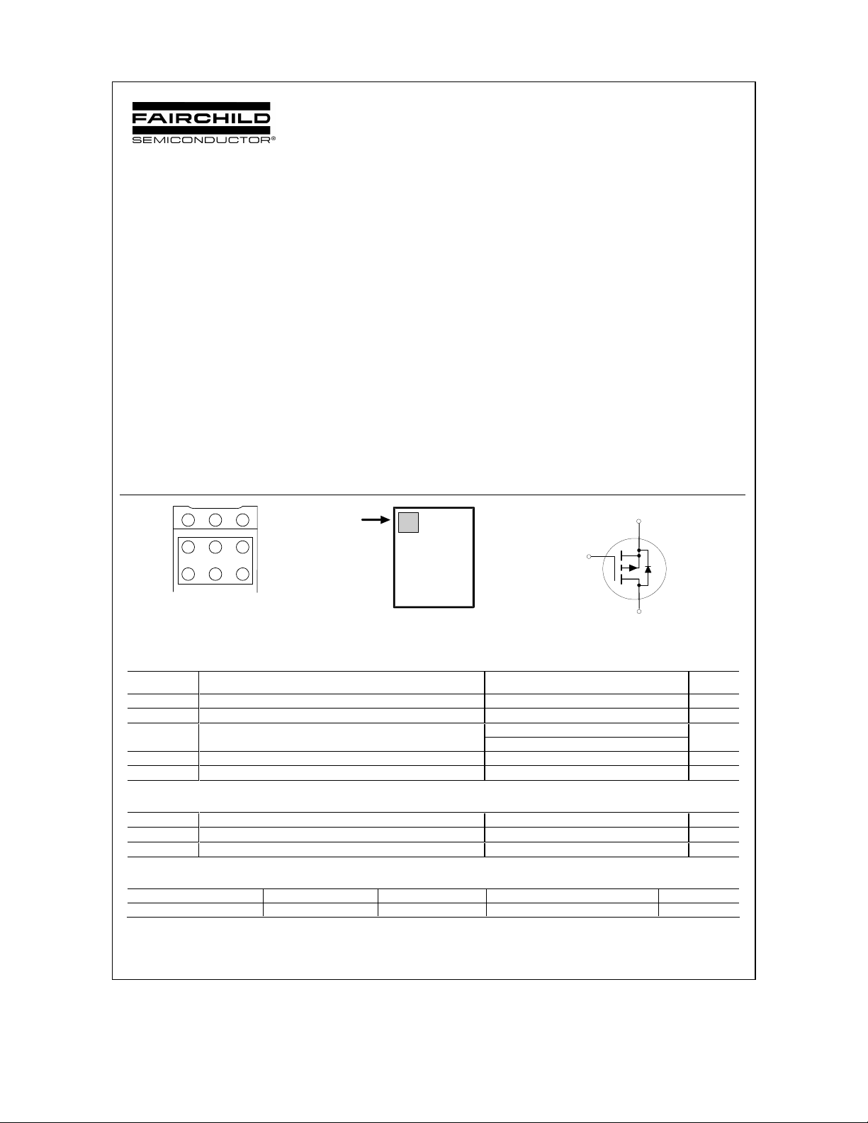
DDD
S
S
G
S
SS
Pin 1
.
Features
• 7.5 A, 20 V. R
R
• Occupies only 4 mm2 of PCB area.
Less than 40% of the area of a SSOT-6
• Ultra-thin package: less than 0.80 mm height when
mounted to PCB
• Ultra-low Qg x R
• High power and current handling capability.
F203N
F203N
= 18 mΩ @ VGS = 4.5
DS(ON)
= 30 mΩ @ VGS = 2.5 V
DS(ON)
figure-of-merit.
DS(ON)
S
G
Bottom
Absolute Maximum Ratings T
Top
o
=25
C unless otherwise noted
A
D
Symbol Parameter Ratings Units
V
Drain-Source Voltage 20 V
DSS
V
Gate-Source Voltage ±12 V
GSS
ID Drain Current – Continuous (Note 1a) 7.5 A
– Pulsed 20
PD Power Dissipation (Steady State) (Note 1a) 1.6 W
TJ, T
Operating and Storage Junction Temperature Range –55 to +150 °C
STG
Thermal Characteristics
R
Thermal Resistance, Junction-to-Ambient (Note 1a) 67 °C/W
θJA
R
Thermal Resistance, Junction-to-Ball (Note 1) 11 °C/W
θJB
R
Thermal Resistance, Junction-to-Case (Note 1) 1 °C/W
θJC
Package Marking and Ordering Information
Device Marking Device Reel Size Tape width Quantity
203N FDZ203N 7’’ 8mm 3000 units
2003 Fairchild Semiconductor Corporation FDZ203N Rev. E2(W)
FDZ203N
Electrical Characteristics T
Symbol
Parameter Test Conditions Min Typ Max Units
= 25°C unless otherwise noted
A
Off Characteristics
BV
Drain–Source Breakdown Voltage VGS = 0 V, ID = 250 µA 20 V
DSS
∆BVDSS
∆TJ
I
Zero Gate Voltage Drain Current VDS = 16 V, VGS = 0 V 1 µA
DSS
I
GSSF
I
GSSR
Breakdown Voltage Temperature
ID = 250 µA, Referenced to 25°C 14 mV/°C
Coefficient
Gate–Body Leakage, Forward VGS = 12 V, VDS = 0 V 100 nA
Gate–Body Leakage, Reverse VGS = –12 V, VDS = 0 V –100 nA
On Characteristics (Note 2)
V
Gate Threshold Voltage VDS = VGS, ID = 250 µA 0.6 0.8 1.5 V
GS(th)
∆VGS(th)
∆TJ
R
DS(on)
I
D(on)
Gate Threshold Voltage
Temperature Coefficient
Static Drain–Source
On–Resistance
ID = 250 µA, Referenced to 25°C
VGS = 4.5 V, ID = 7.5 A
VGS = 2.5 V, ID = 5.5 A
VGS = 4.5 V, ID = 7.5 A, TJ=125°C
–3 mV/°C
14
20
20
28
18
30
On–State Drain Current VGS = 4.5 V, VDS = 5 V 20 A
gFS Forward Transconductance VDS = 10 V, ID = 7.5 A 33 S
Dynamic Characteristics
C
Input Capacitance 1127 pF
iss
C
Output Capacitance 268 pF
oss
C
Reverse Transfer Capacitance
rss
VDS = 10 V, V
f = 1.0 MHz
= 0 V,
GS
134 pF
Switching Characteristics (Note 2)
t
Turn–On Delay Time 8 16 ns
d(on)
tr Turn–On Rise Time 11 20 ns
t
Turn–Off Delay Time 26 42 ns
d(off)
tf Turn–Off Fall Time
Qg Total Gate Charge 11 15 nC
Qgs Gate–Source Charge 2 nC
Qgd Gate–Drain Charge
VDD = 10V, ID = 1 A,
VGS = 4.5 V, R
GEN
= 6 Ω
VDS = 10 V, ID = 7.5 A,
VGS = 4.5 V
8 16 ns
3 nC
Drain–Source Diode Characteristics and Maximum Ratings
IS Maximum Continuous Drain–Source Diode Forward Current 1.3 A
VSD Drain–Source Diode Forward
Voltage
trr Diode Reverse Recovery Time 20 nS
Qrr Diode Reverse Recovery Charge
Notes:
1. R
is determined with the device mounted on a 1 in² 2 oz. copper pad on a 1.5 x 1.5 in. board of FR-4 material. The thermal resistance from the junction to
θJA
the circuit board side of the solder ball, R
copper chip carrier. R
θJC
and R
θJB
, is defined for reference. For R
θJB
are guaranteed by design while R
VGS = 0 V, IS = 1.3 A (Note 2) 0.7 1.2 V
IF = 9A,
diF/dt = 100 A/µs
, the thermal reference point for the case is defined as the top surface of the
θJC
is determined by the user's board design.
θJA
14 nC
mΩ
a) 67 °C/W when
mounted on a 1in2 pad
of 2 oz copper, 1.5” x
1.5” x 0.062” thick
PCB
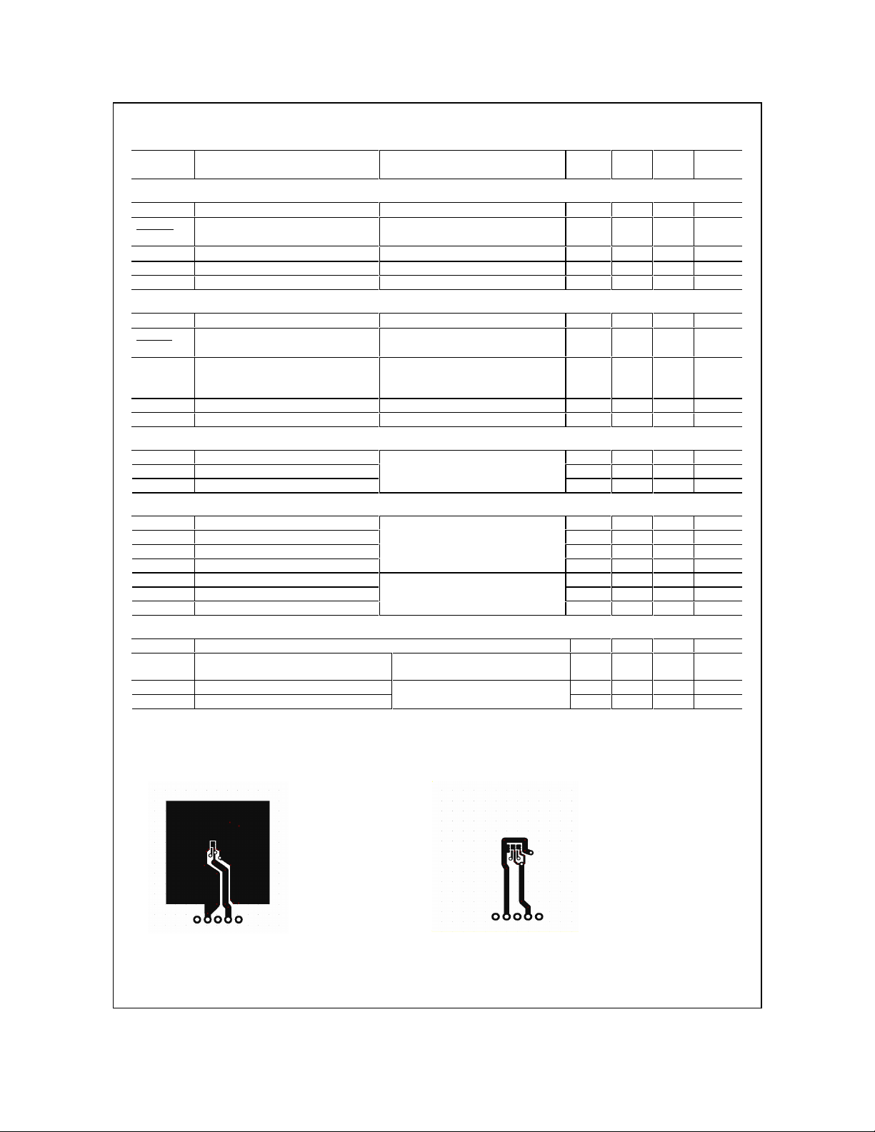
Scale 1 : 1 on letter size paper
2. 2. Pulse Test: Pulse Width < 300µs, Duty Cycle < 2.0%
b) 155 °C/W when mounted
on a minimum pad of 2 oz
copper
FDZ203N Rev. E2 (W)
 Loading...