

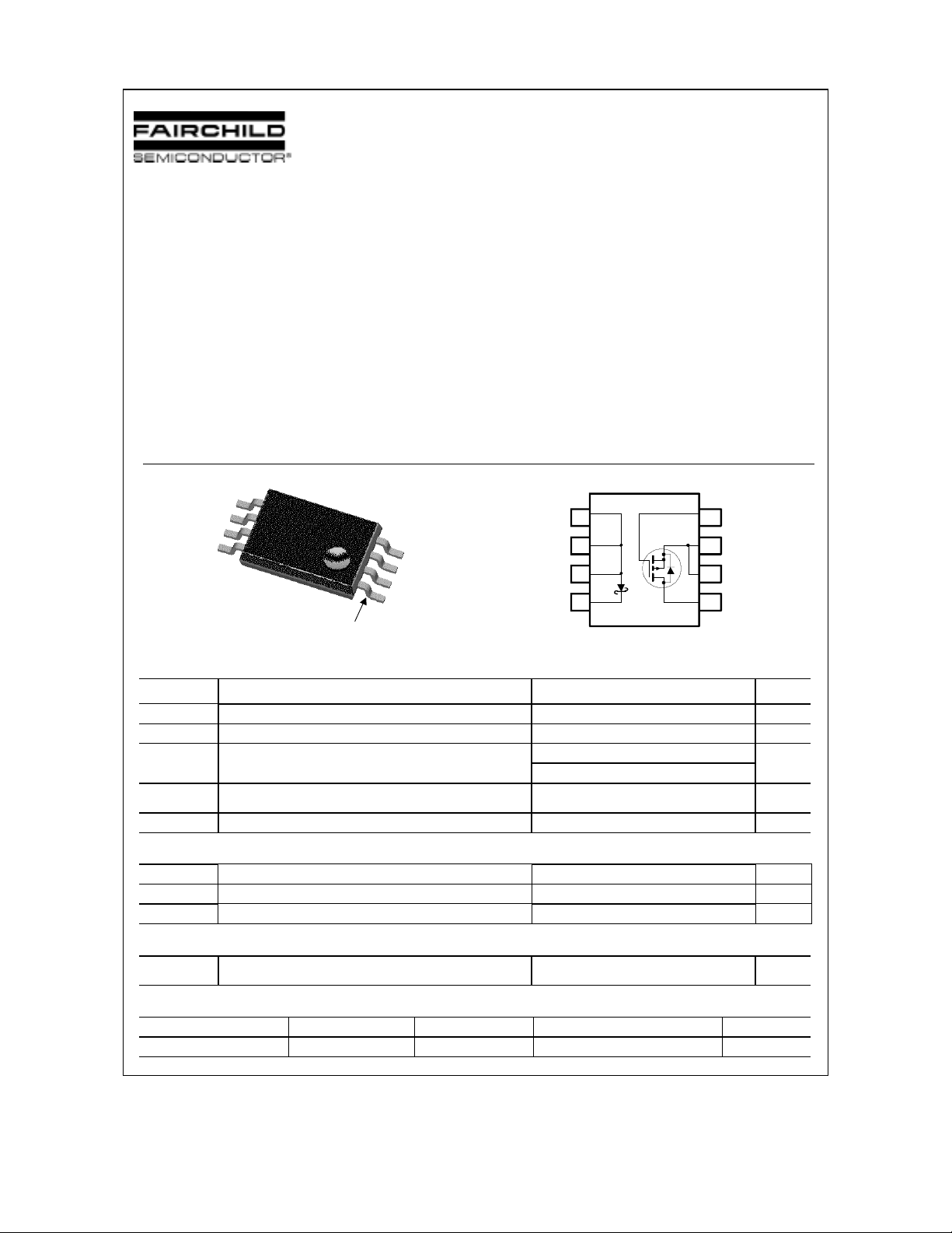
Fairchild Semiconductor FDW6923 Datasheet
May 2002
FDW6923
P-Channel 2.5V Specified PowerTrench
MOSFET with Schottky Diode
FDW6923
General Description
This P-Channel 2.5V specified MOSFET is a rugged
gate version of Fairchild Semiconductor’s advanced
PowerTrench process. It is combined with a low
forward drop Schottky diode which is isolat ed from the
MOSFET, providing a compact power solution for
asynchronous DC/DC converter appli cations.
Applications
• DC/DC conversion
A
A
A
C
G
S
S
D
TSSOP-8
Pin 1
MOSFET Absolute Maximum Ratings T
Features
• –3.5 A, –20 V. R
R
• V
< 0.55 V @ 1 A
F
• High performance trench te chnology for extremely
low R
• Low profile TSSOP-8 package
DS(ON)
5
6
7
8
= 0.045 Ω @ VGS = –4.5 V
DS(ON)
= 0.075 Ω @ VGS = –2.5 V
DS(ON)
4
3
2
1
o
=25
C unless otherwise noted
A
Symbol Parameter Ratings Units
V
Drain-Source Voltage
DSS
V
Gate-Source Voltage
GSS
ID Drain Current – Continuous (Note 1)
– Pulsed
PD
TJ, T
STG
MOSFET Power Dissipation (minimum pad)
Schottky Power Dissi pation (minimum pad)
Operating and Storage Junction Temperature Range -55 to +150
(Note 1)
(Note 1)
–20
± 12
–3.5
–30
1.2
1.0
V
V
A
W
°C
Schottky Maximum Ratings
V
Repetitive Peak Reverse Volt age 20 V
RRM
IF Average Forward Current 1.5 A
IFM Peak Forward Current 30 A
Thermal Characteristics
R
θJA
Thermal Resistance, Junction-to-Ambient
(minimum pad)
(Note 1)
MOSFET: 115
Schottky: 130
Package Marking and Ordering Information
Device Marking Device Reel Size Tape width Quantity
6923 FDW6923 13’’ 16mm 3000 units
2002 Fairchild Semiconductor International
FDW6923 Rev . D(W)
°C/W
FDW6923
Electrical Characteristics T
= 25°C unless otherwise noted
A
Symbol Parameter Test Conditions Min Typ Max Units
Off Characteristics
BV
Drain–Source Breakdown Voltage
DSS
∆BVDSS
∆T
I
Zero Gate Voltage Drain Current VDS = –16 V, VGS = 0 V –1
DSS
I
GSSF
I
GSSR
Breakdown Voltage Temperature
Coefficient
J
Gate–Body Leakage, Forward VGS = –12 V, VDS = 0 V –100 nA
Gate–Body Leakage, Reverse VGS = 12 V, VDS = 0 V 100 nA
V
= 0 V, ID = –250 µA
GS
= –250 µA, Referenced to25°C
I
D
–20 V
–16
mV/°C
µA
On Characteristics (Note 2)
V
Gate Threshold Voltage
GS(th)
∆VGS(th)
∆TJ
R
DS(on)
Gate Threshold Voltage
Temperature Coefficient
Static Drain–Source
On–Resistance
I
On–State Drain Current VGS = –4.5 V, VDS = –5 V –15 A
D(on)
V
= VGS, ID = –250 µA
DS
= –250 µA, Referenced to25°C
I
D
V
= –4.5 V, ID = –3.5 A
GS
= –2.5 V, ID = –2.7 A
V
GS
=–4.5 V, ID =–3.5A, TJ=125°C
V
GS
–0.6 –1.0 –1.5 V
3
36
56
49
45
75
72
mV/°C
mΩ
gFS Forward Transconductance VDS = –5 V, ID = –3.5A 13.2 S
Dynamic Characteristics
C
Input Capacitance 1030 pF
iss
C
Output Capacitance 280 pF
oss
C
Reverse Transfer Capacitance
rss
= –10 V, V
V
DS
f = 1.0 MHz
= 0 V,
GS
120 pF
Switching Characteristics (Note 2)
t
Turn–On Delay Time 11 20 ns
d(on)
tr Turn–On Rise Time 18 32 ns
t
Turn–Off Delay Time 34 55 ns
d(off)
tf Turn–Off Fall Time
Qg Total Gate Charge 9.7 16 nC
Qgs Gate–Source Charge 2.2 nC
Qgd Gate–Drain Charge
= –5 V, ID = –1 A,
V
DD
= –4.5 V, R
V
GS
V
= –5V, ID = –3.5 A,
DS
= –4.5 V
V
GS
GEN
= 6 Ω
34 55 ns
2.4 nC
Drain–Source Diode Characteristics and Maximum Ratings
IS Maximum Continuous Drain–Source Diode Forward Current –1.25 A
VSD Drain–Source Diode Forward
VGS = 0 V, IS = –1.25 A (Note 2) –0.6 –1.2 V
Voltage
I
Gate–Body Leakage, Reverse VGS = 12 V, VDS = 0 V 100 nA
GSSR
Schottky Diode Characteristics
IR Reverse Leakage VR = 20V
VF Forward Voltage IF = 1A
TJ=25°C
T
=125°C
J
TJ=25°C
T
=125°C
J
CT Junction Capacitance VR = 10V 50 pF
Notes:
1. R
is the sum of the junction-to-case and case-to-ambient thermal resistance where the case thermal reference is defined as the so lder mounting surface of
θJA
the drain pins. R
R
is 115 °C/W for the MOSFET and 130°C/W for the Schottky Diode when mounted on a minimum pad.
θJA
2. Pulse Test: Pulse Width < 300µs, Duty Cycle < 2.0%
is guaranteed by design while R
θJC
is determined by the user's board design.
θCA
0.6 50
1 8 mA
0.48 0.55 V
0.42 0.50 V
FDW6923 Rev . D (W)
µA
 Loading...