

Fairchild Semiconductor FDW2521C Datasheet
May 2002
FDW2521C
Complementary PowerTrench
MOSFET
FDW2521C
General Description
This complementary MOSFET device is produced using
Fairchild’s advanced PowerTrench process that has
been especially tailored to minimize the on-state
resistance and yet maintain low gate charge for
superior switching performance.
Applications
• DC/DC conversion
• Power management
• Load switch
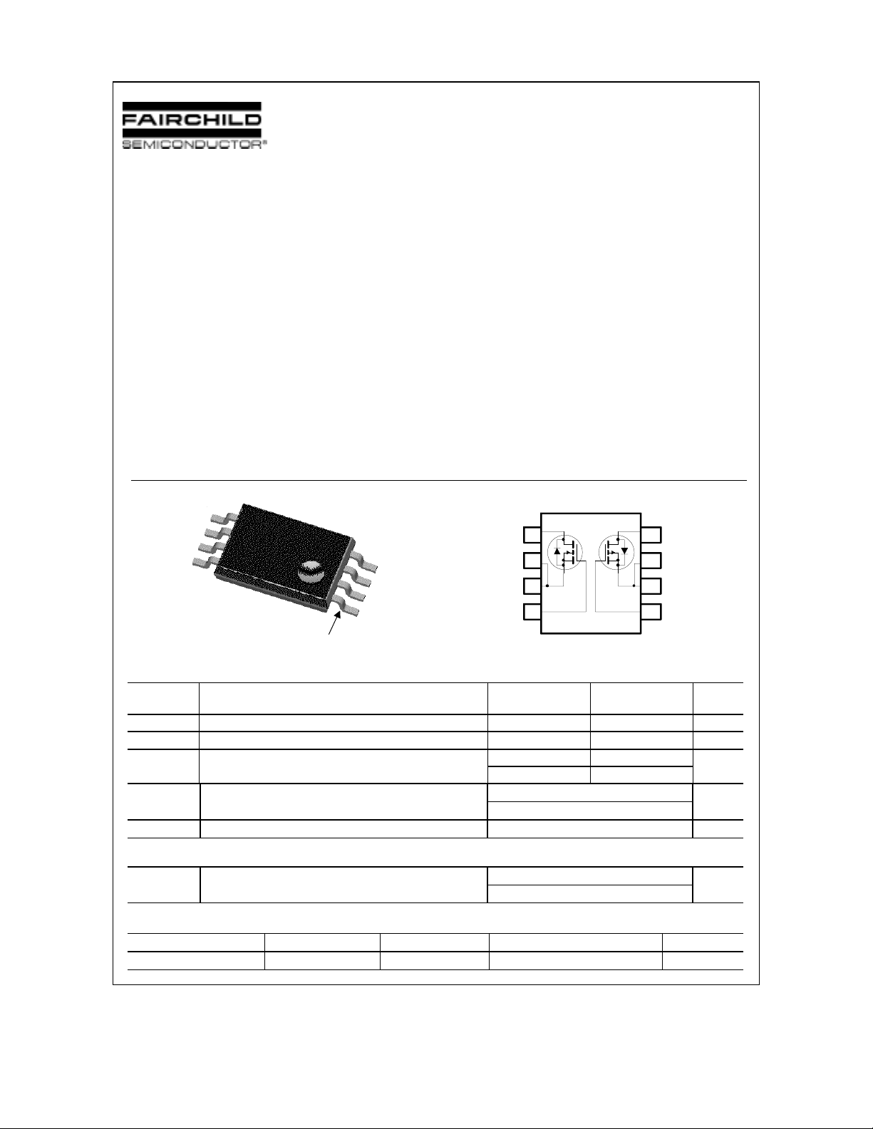
G
2
S
2
S
2
D
2
G
1
S
1
S
1
D
1
TSSOP-8
Pin 1
Absolute Maximum Ratings T
= 25°C unless otherwise noted
A
Features
• Q1: N-Channel
5.5 A, 20 V. R
R
= 21 mΩ @ VGS = 4.5 V
DS(ON)
= 35 mΩ @ VGS = 2.5 V
DS(ON)
• Q2: P-Channel
–3.8 A, 20 V. R
R
= 43 mΩ @ VGS = –4.5 V
DS(ON)
= 70 mΩ @ VGS = –2.5 V
DS(ON)
• High performance trench te chnology for extremely
DS(ON)
low R
• Low profile TSSOP-8 package
1
2
3
4
Q1 Q2
8
7
6
5
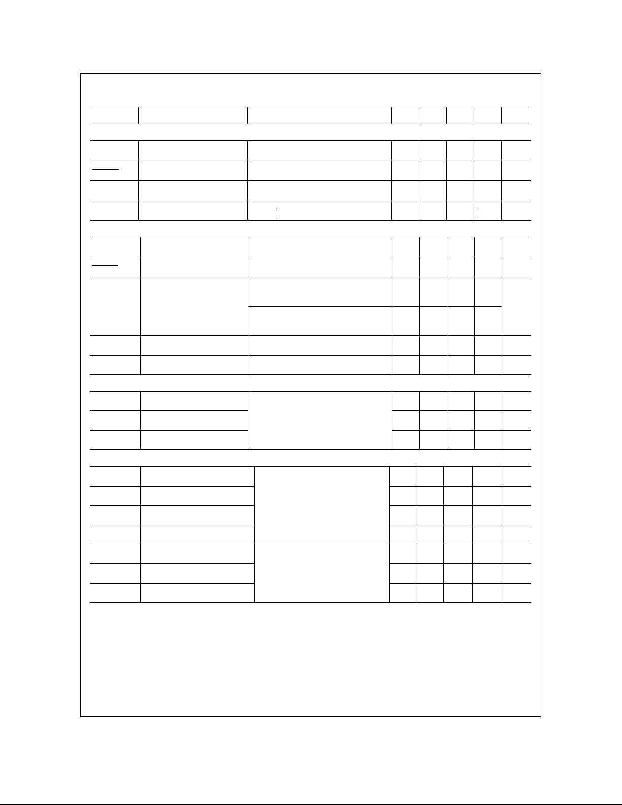
Symbol Parameter Q1 Q2 Units
V
Drain-Source Voltage 20 –20 V
DSS
V
Gate-Source Voltage
GSS
±12 ±12
V
ID Drain Current - Continuous (Note 1a) 5.5 –3.8 A
- Pulsed 30 –30
PD Power Dissipation (Note 1a) 1.0 W
TJ, T
STG
Operating and Storage Junction Temperature Range -55 to +150
(Note 1b)
0.6
°C
Thermal Characteristics
R
θJA
Thermal Resistance, Junction-to-Ambient
(Note 1a) 125
(Note 1b)
208
°C/W
Package Marking and Ordering Information
Device Marking Device Reel Size Tape width Quantity
2521C FDW2521C 13’’ 12mm 3000 units
2002 Fairchild Semiconductor Corporation
FDW2521C Rev D( W)
FDW2521C
Electrical Characteristics T
= 25°C unless otherwise noted
A
Symbol Parameter Test Conditions Type Min Typ Max Units
Off Characteristics
BV
Drain-Source Breakdown
DSS
Voltage
∆BVDSS
∆T
J
I
Zero Gate Voltage Drain
DSS
Breakdown Voltage
Temperature Coefficient
Current
I
Gate-Body Leakage VGS = +12 V, VDS = 0 V
GSS
VGS = 0 V, ID = 250 µA
V
= 0 V, ID = –250 µA
GS
I
= 250 µA, Referenced to 25°C
D
= –250 µA, Referenced to 25°C
I
D
VDS = 16 V, VGS = 0 V
V
= –16 V, VGS = 0 V
DS
= +12 V, VDS = 0 V
V
GS
Q1
Q2
–20
Q1
Q2
Q1
Q2
Q1
Q2
20
V
14
–16
1
–1
+
+
100
100
mV/°C
µA
nA
On Characteristics (Note 2)
Q1
0.6
0.8
V
Gate Threshold Voltage VDS = VGS, ID = 250 µA
GS(th)
∆VGS(th)
∆TJ
R
DS(on)
Gate Threshold Voltage
Temperature Coefficient
Static Drain-Source
On-Resistance
V
I
On-State Drain Current VGS = 4.5 V, VDS = 5 V
D(on)
= VGS, ID = –250 µA
V
DS
= 250 µA, Referenced to 25°C
I
D
= –250 µA, Referenced to 25°C
I
D
VGS = 4.5 V, ID = 5.5 A
V
= 2.5 V, ID = 4.2 A
GS
= 4.5 V, ID = 5.5 A, TJ = 125°C
V
GS
= –4.5 V, ID = –3.8 A
GS
= –2.5 V, ID = –3.0 A
V
GS
= –4.5 V, ID = –3.8 A, TJ = 125°C
V
GS
= –4.5 V, VDS = –5 V
V
GS
gFS Forward Transconductance VDS = 5 V, ID = 5.5 A
V
= –5 V, ID = –3.5 A
DS
Q2
–0.6
Q1
–3.2
Q2
Q1
17
Q2 36
Q1
30
Q2
–15
Q1
26
Q2
1.5
–1.0
–1.5 V
mV/°C
3.0
21
24
23
mΩ
35
34
43
56
70
49
69
A
S
13.2
Dynamic Characteristics
C
Input Capacitance Q1
iss
C
Output Capacitance Q1
oss
C
Reverse Transfer
rss
Capacitance
Q1:
V
= 10 V, VGS = 0 V,
DS
f = 1.0 MHz
Q2:
= –10 V, VGS = 0 V,
V
DS
f = 1.0 MHz
Q2
Q2
Q1
Q2
1082
1030
277
280
130
120
pF
pF
pF
Switching Characteristics
t
Turn-On Delay Time
d(on)
tr Turn-On Rise Time
t
Turn-Off Delay Time
d(off)
tf Turn-Off Fall Time
Qg Total Gate Charge
Qgs Gate-Source Charge
Qgd Gate-Drain Charge
Q1:
VDD = 10 V, ID = 1 A,
= 4.5 V, R
V
GS
GEN
= 6 Ω
Q2:
V
= –5 V, ID = –1 A,
DD
= –4.5V, R
V
GS
GEN
= 6 Ω
Q1:
= 10 V, ID = 5.5 A, VGS = 4.5 V
V
DS
Q2:
= –5 V, ID = –3.8 A,VGS = –4.5 V
V
DS
Q1
Q2
Q1
Q2
Q1
Q2
Q1
Q2
Q1
Q2
Q1
Q2
Q1
Q2
8
11
8
18
24
34
8
34
12
9.7
2
2.2
3
2.4
20
20
27
32
38
55
16
55
17
nC
16
nC
nC
ns
ns
ns
ns
FDW2521C Rev D( W)
Electrical Characteristics (continued) T
= 25°C unless otherwise noted
A
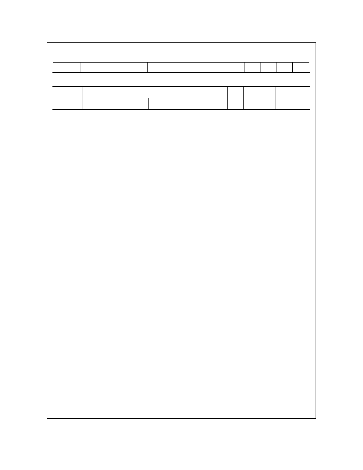
Symbol Parameter Test Conditions Type Min Typ Max Units
Drain-Source Diode Characteristics and Maximum Ratings
IS Maximum Continuous Drain-Source Diode Forward Current Q1
VSD Drain-Source Diode Forward
Voltage
Notes:
1. R
is the sum of the junction-to-case and case-to-ambient thermal resistance where the case thermal reference is defined as the solder mounting surface of
θJA
the drain pins. R
a) R
is 125°C/W (steady state) when mounted on a 1 inch² copper pad on FR-4.
θJA
is 208°C/W (steady state) when mounted on a minimum copper pad on FR-4.
b) R
θJA
2. Pulse Test: Pulse Width < 300µs, Duty Cycle < 2.0%
is guaranteed by design while R
θJC
VGS = 0 V, IS = 0.83 A (Note 2)
VGS = 0 V, IS = –0.83 A (Note 2)
is determined by the user's board design.
θCA
0.83
Q2
Q1
Q2
0.7
–0.7
–0.83 A
1.2
–1.2 V
FDW2521C
FDW2521C Rev D( W)
 Loading...