

Fairchild Semiconductor FDW2507N Datasheet
March 2003
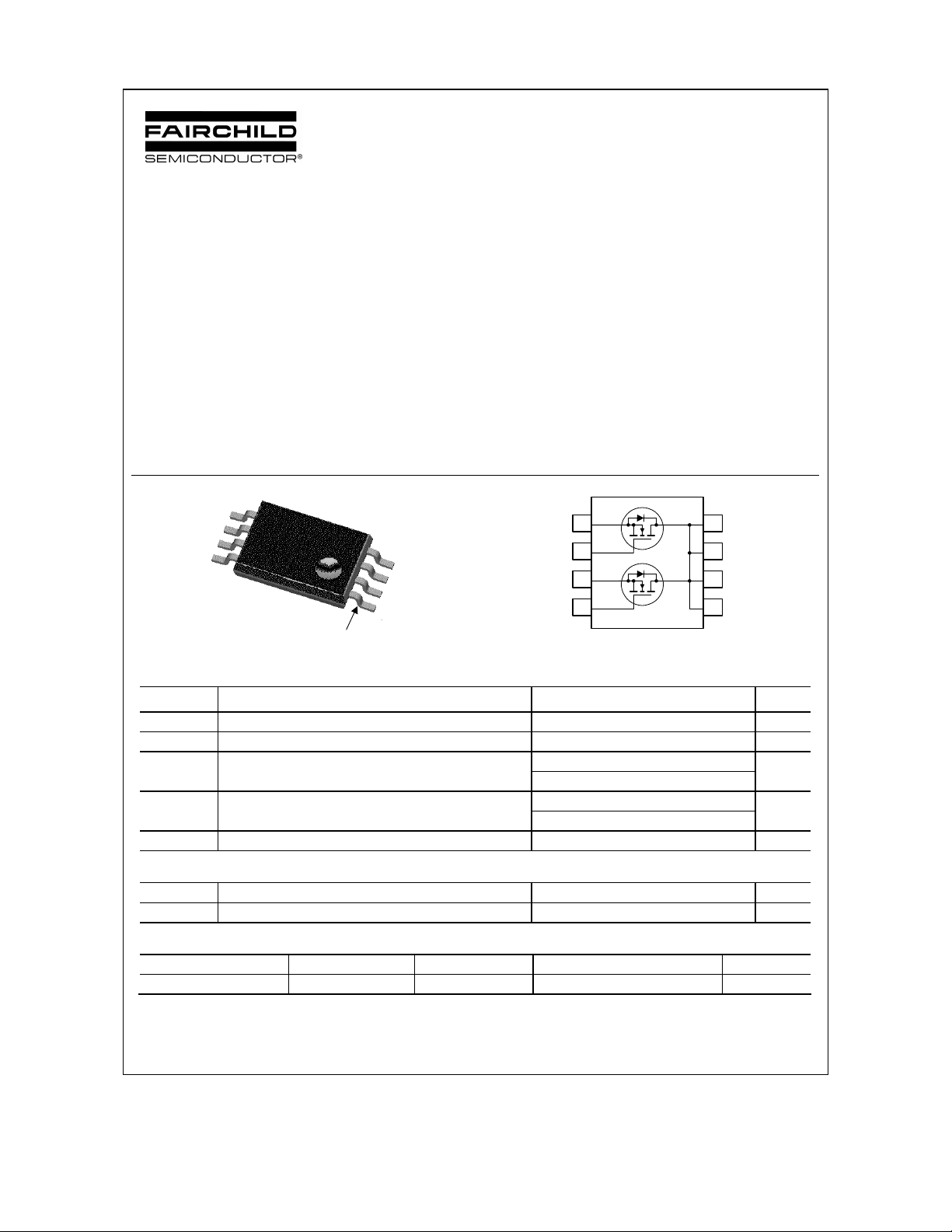
FDW2507N
Common Drain N-Channel 2.5V specified PowerTrench
MOSFET
FDW2507N
General Description
This monolithic common drain N-Channel MOSFET has
been designed using Fairchild Semiconductor’s
advanced PowerTrench process to optimize the R
= 2.5v on special TSSOP-8 lead frame with all
@ V
GS
DS(ON)
the drains on one side of the package.
Applications
• Li-Ion Battery Pack
Features
• 7.5 A, 20 V. R
R
• Isolated source and drain pins
• High performance trench technology for extremely
low R
@ VGS = 2.5 V
DS(ON)
= 19 mΩ @ VGS = 4.5 V
DS(ON)
= 23 mΩ @ VGS = 2.5 V
DS(ON)
• Low profile TSSOP-8 package
D
D
D
D
S
TSSOP-8
Pin 1
Absolute Maximum Ratings
G
2
S
2
G
1
1
TA=25oC unless otherwise noted
81
72
63
54
Symbol Parameter Ratings Units
V
Drain-Source Voltage 20 V
DSS
V
Gate-Source Voltage
GSS
ID Drain Current – Continuous
(Note 1a)
7.5 A
±
12
– Pulsed 30
PD
Power Dissipation for Single Operation
TJ, T
Operating and Storage Junction Temperature Range –55 to +150
STG
(Note 1a)
1.6
(Note 1b)
1.1
V
W
°
C
Thermal Characteristics
R
θJA
R
θJA
Thermal Resistance, Junction-to-Ambient
Thermal Resistance, Junction-to-Ambient
(Note 1a)
(Note 1b)
77
114
Package Marking and Ordering Information
Device Marking Device Reel Size Tape width Quantity
2003 Fairchild Semiconductor Corporation
2507N FDW2507N 13’’ 12mm 3000 units
°
C/W
°
C/W
FDW2507N Rev C2
FDW2507N
Electrical Characteristics
TA = 25°C unless otherwise noted
Symbol Parameter Test Conditions Min Typ Max Units
Off Characteristics
BV
DSS
∆
BV
∆
T
I
Zero Gate Voltage Drain Current VDS = 16 V, VGS = 0 V 1
DSS
I
GSSF
I
GSSR
On Characteristics
V
GS(th)
∆
V
GS(th)
∆
TJ
R
DS(on)
Drain–Source Breakdown Voltage
DSS
Breakdown Voltage Temperature
Coefficient
J
Gate–Body Leakage, Forward VGS = 12 V, VDS = 0 V 100 nA
Gate–Body Leakage, Reverse VGS = –12 V, VDS = 0 V –100 nA
(Note 2)
Gate Threshold Voltage
Gate Threshold Voltage
Temperature Coefficient
Static Drain–Source
On–Resistance
I
On–S t at e Drain Current VGS = 4.5 V, VDS = 5 V 30 A
D(on)
= 0 V, ID = 250 µA
V
GS
= 250 µA, Referenced to 25°C
I
D
= VGS, ID = 250 µA
V
DS
I
= 250 µA, Referenced to 25°C
D
VGS = 4.5 V, ID = 7.5 A
V
= 2.5 V, ID = 6.8 A
GS
V
= 4.5 V, ID = 7.5 A, TJ=125°C
GS
gFS Forward Transconductance VDS = 5 V, ID = 7.5 A 31 S
20 V
–13
mV/°C
µ
A
0.6 0.8 1.5 V
4
15
17
20
19
23
27
mV/
m
°
C
Ω
Dynamic Characteristics
C
Input Capacitance 2152 pF
iss
C
Output Capacitance 512 pF
oss
C
Reverse Transfer Capacitance
rss
Switching Characteristics
t
Turn–On Delay Time 12 22 ns
d(on)
(Note 2)
tr Turn–On Rise Time 13 23 ns
t
Turn–Off Delay Time 35 56 ns
d(off)
tf Turn–Off Fall Time
Qg Total Gate Charge 20 28 nC
Qgs Gate–Source Charge 3 nC
Qgd Gate–Drain Charge
= 10 V, V
V
DS
f = 1.0 MHz
V
= 10 V, ID = 1 A,
DD
= 4.5 V, R
V
GS
V
= 10 V, ID = 7.5 A,
DS
= 4.5 V
V
GS
= 0 V,
GS
= 6 Ω
GEN
263 pF
19 34 ns
5 nC
Drain–Source Diode Characteristics and Maximum Ratings
IS Maximum Continuous Drain–Source Diode Forward Current 1.3 A
VSD
trr Diode Reverse Recovery Time 26 nS
Qrr Diode Reverse Recovery Charge
Notes:
1. R
is the sum of the junction-to-case and case-to-ambient thermal resistance where the case thermal reference is defined as the solder mounting surface of
θJA
the drain pins. R
2. Pulse Test: Pulse Width < 300µs, Duty Cycle < 2.0%
Drain–Source Diode Forward
Voltage
is guaranteed by design while R
θJC
θCA
a) 77°C/W when
mounted on a 1in
of 2 oz copper
VGS = 0 V, IS = 1.3 A
= 7.5A
I
F
= 100 A/µs
d
iF/dt
is determined by the user's board design.
2
pad
(Note 2)
0.6 1.2 V
(Note 2)
21 nC
b) 114°C/W when mounted
on a minimum pad of 2 oz
copper
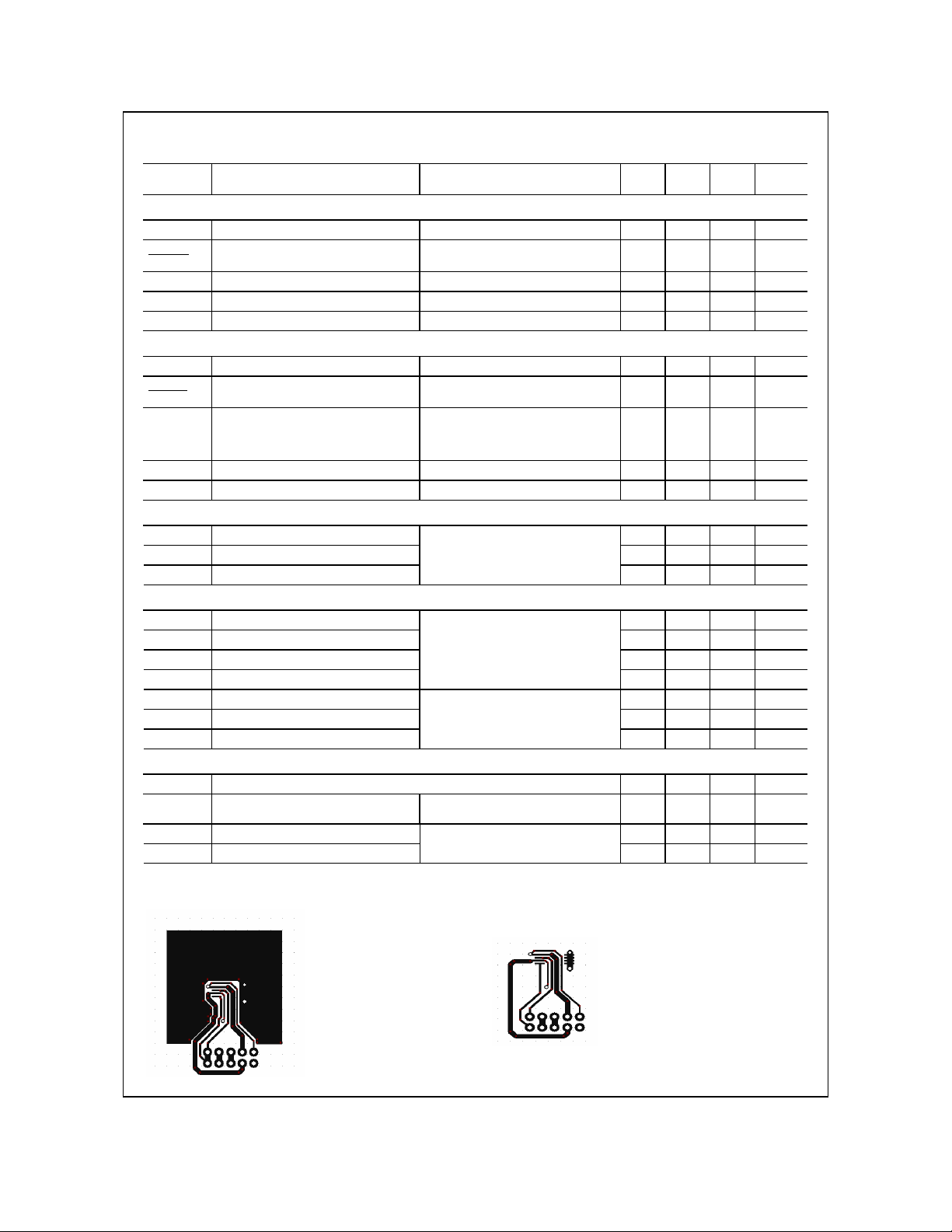
Scale 1 : 1 on letter size paper
FDW2507N Rev C2
 Loading...