

Fairchild Semiconductor FDW2502PZ Datasheet
FDW2502PZ
FDW2502PZ
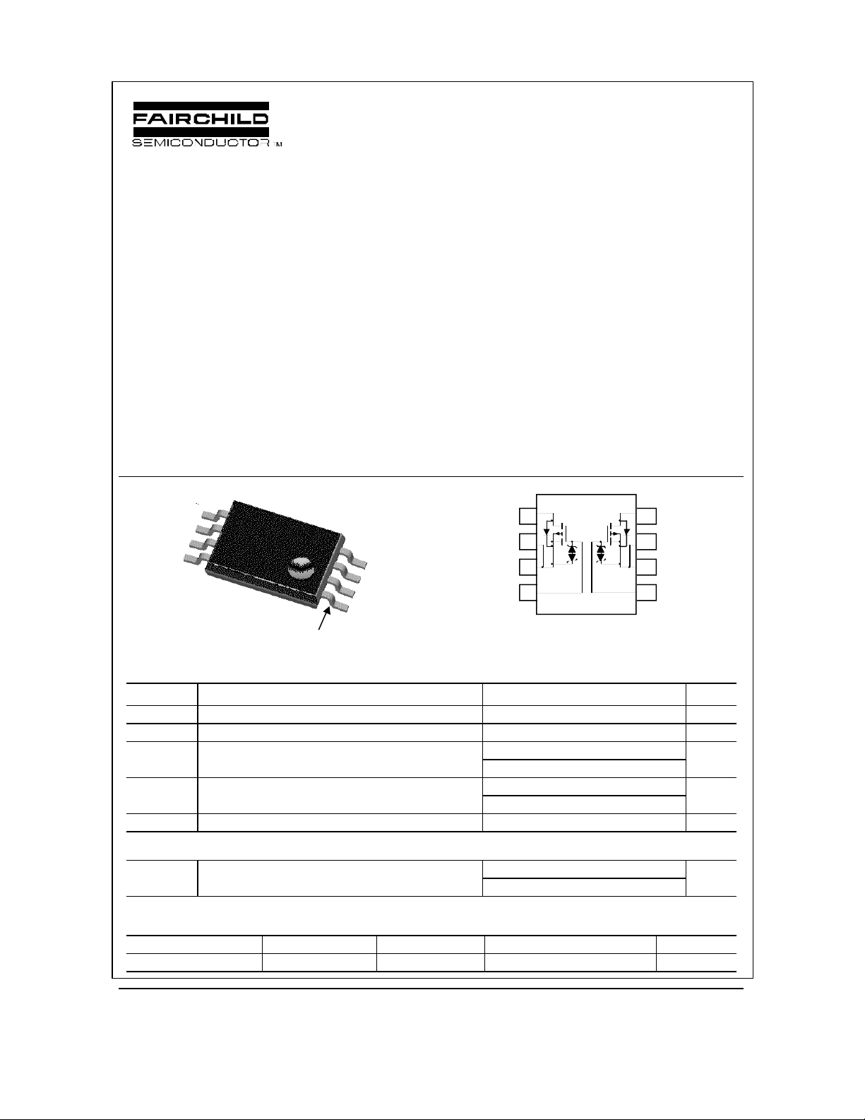
Dual P-Channel 2.5V Specified PowerTrench MOSFET
March 2000
PRELIMINARY
General Description
This P-Channel 2.5V specified MOSFET is a rugged
gate version of Fairchild's Semiconductor’s advanced
PowerTrench process. It has been optimized for power
management applications with a wide range of gate
drive voltage (2.5V –12V).
Applications
• Load switch
• Motor drive
• DC/DC conversion
• Power management
G2
S2
S2
D2
G1
S1
S1
D1
TSSOP-8
Pin 1
Features
• –4.4 A, –20 V.R
• Extended V
GSS
• ESD protection diode (note 3).
• High performance trench technology for extremely
low R
DS(ON)
.
• Low profile TSSOP-8 package.
1
2
3
4
= 0.035 Ω @ VGS = –4.5 V
DS(ON)
R
= 0.057 Ω @ VGS = –2.5 V.
DS(ON)
range (±12V) for battery applications.
8
7
6
5
Absolute Maximum Ratings T
=25oC unless otherwise noted
A
Symbol Parameter Ratings Units
V
DSS
V
GSS
I
D
P
D
TJ, T
STG
Drain-Source Voltage –20 V
Gate-Source Voltage ±12 V
Drain Current – Continuous (Note 1a) –4.4 A
– Pulsed –30
Power Dissipation for Single Operation (Note 1a) 1.0 W
(Note 1b)
0.6
Operating and Storage Junction Temperature Range -55 to +150 °C
Thermal Characteristics
R
θJA
Thermal Resistance, Junction-to-Ambient (Note 1a) 125 °C/W
(Note 1b)
208
Package Marking and Ordering Information
Device Marking Device Reel Size Tape width Quantity
2502PZ FDW2502PZ 13’’ 12mm 3000 units
2000 Fairchild Semiconductor Corporation
FDW2502PZ Rev. B (W)
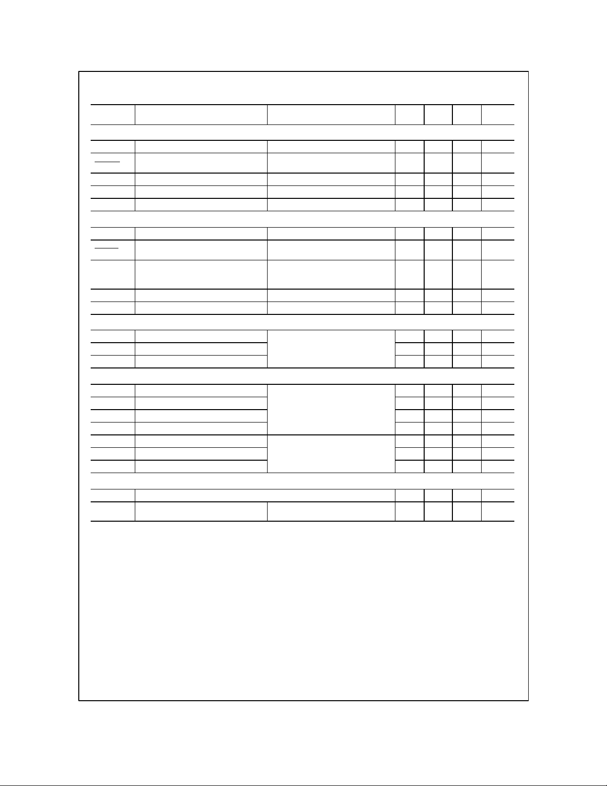
Electrical Characteristics T
0.028
0.043
0.035
0.057
FDW2502PZ
= 25°C unless otherwise noted
A
Symbol Parameter Test Conditions Min Typ Max Units
Off Characteristics
BV
DSS
∆BVDSS
∆T
J
I
DSS
I
GSSF
I
GSSR
Drain–Source Breakdown Voltage
Breakdown Voltage Temperature
Coefficient
Zero Gate Voltage Drain Current VDS = –16 V, VGS = 0 V –1
Gate–Body Leakage, Forward VGS = –12 V, VDS = 0 V –10
Gate–Body Leakage, Reverse VGS = 12 V VDS = 0 V 10
VGS = 0 V, ID = –250 µA
ID = –250 µA, Referenced to 25°C
–20 V
–17
mV/°C
µA
µA
µA
On Characteristics (Note 2)
V
GS(th)
∆VGS( th)
∆T
R
DS(on)
I
D(on)
g
FS
Gate Threshold Voltage VDS = VGS, ID = –250 µA –0.4 -1.0 –1.5 V
Gate Threshold Voltage
Temperature Coefficient
J
Static Drain–Source
On–Resistance
ID = –250 µA, Referenced to 25°C 3.1 mV/°C
VGS = –4.5 V, ID = –4.4 A
VGS = –4.5 V, ID = –4.4 ,TJ=125°C
0.039
VGS = –2.5 V, ID = –3.3 A
On–State Drain Current VGS = –4.5 V, VDS = –5 V –30 A
Forward Transconductance VDS = –5 V, ID = –4.4 A 17 S
0.056
Ω
Dynamic Characteristics
C
iss
C
oss
C
rss
Input Capacitance 1330 pF
Output Capacitance 552 pF
Reverse Transfer Capacitance
VDS = –10 V, V
f = 1.0 MHz
GS
= 0 V,
153 pF
Switching Characteristics (Note 2)
t
t
t
t
Q
Q
Q
d(on)
r
d(off)
f
g
gs
gd
Turn–On Delay Time 12 25 ns
Turn–On Rise Time 19 40 ns
Turn–Off Delay Time 60 100 ns
Turn–Off Fall Time
Total Gate Charge 14 20 nC
Gate–Source Charge 3.0 nC
Gate–Drain Charge
VDD = –10 V, ID = –1 A,
VGS = –4.5 V, R
GEN
= 6 Ω
VDS = –5 V, ID = –4.4 A,
VGS = –4.5 V
37 70 ns
3.9 nC
Drain–Source Diode Characteristics and Maximum Ratings
I
S
V
SD
Notes:
1. R
θJA
the drain pins. R
a) R
b) R
2. Pulse Test: Pulse Width < 300µs, Duty Cycle < 2.0.
3. The diode connected between the gate and source serves only as protection against ESD. No gate overvoltage rating is implied.
Maximum Continuous Drain–Source Diode Forward Current –0.83 A
Drain–Source Diode Forward
Voltage
is the sum of the junction-to-case and case-to-ambient thermal resistance where the case thermal reference is defined as the solder mounting surface of
θJA
θJA
is guaranteed by design while R
θJC
is 125°/W (steady state) when mounted on 1 inch² copper pad on FR-4.
is 250°/W (steady state) when mounted on minimum copper pad on FR-4.
θCA
VGS = 0 V, IS = –0.83 A (Note 2) -0.7 –1.2 V
is determined by the user's board design.
FDW2502PZ Rev. B (W)
 Loading...