

Fairchild Semiconductor FDV302P Datasheet
October 1997
FDV302P
Digital FET, P-Channel
General Description Features
This P-Channel logic level enhancement mode field effect
transistor is produced using Fairchild's proprietary, high cell
density, DMOS technology. This very high density process is
especially tailored to minimize on-state resistance. This
device has been designed especially for low voltage
applications as a replacement for digital transistors. Since
bias resistors are not required, this one P-channel FET can
replace several digital transistors with different bias resistors
such as the DTCx and DCDx series.
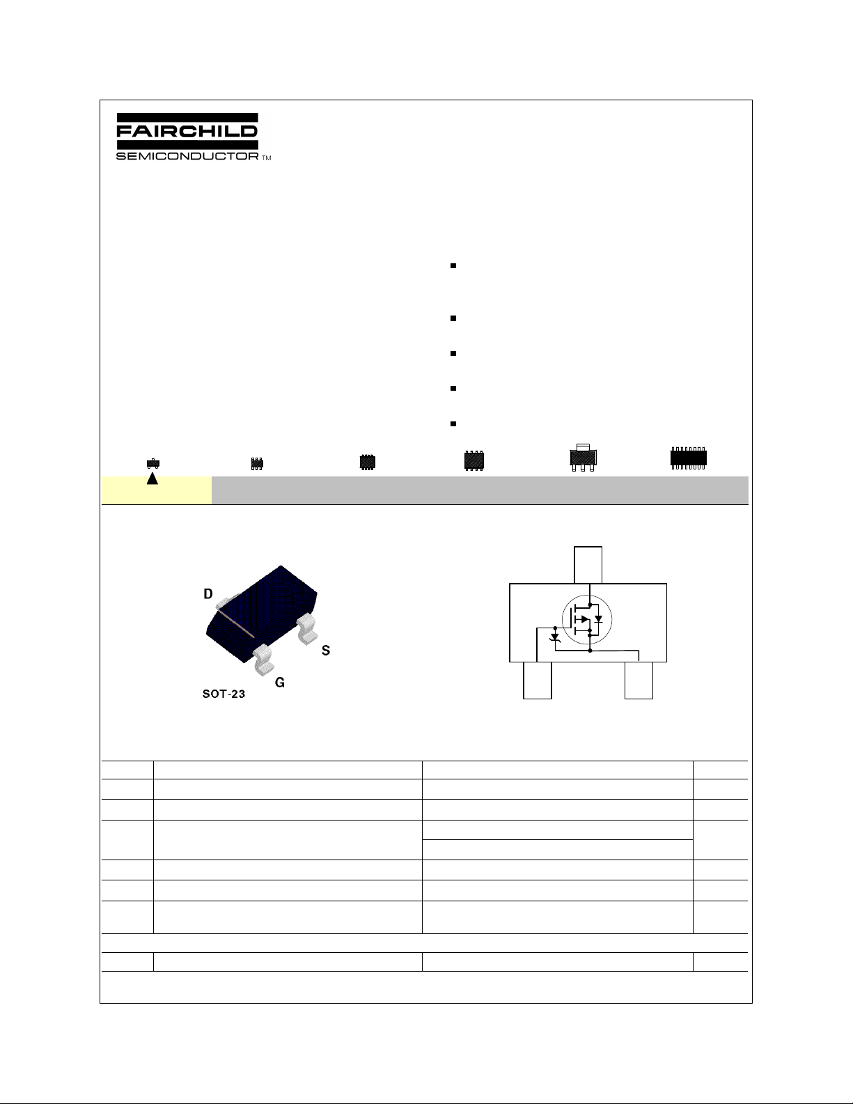
SOT-23
Mark:302
SuperSOTTM-6
SuperSOTTM-8
-25 V, -0.12 A continuous, -0.5 A Peak.
R
= 13 Ω @ VGS= -2.7 V
DS(ON)
R
= 10 Ω @ V
DS(ON)
= -4.5 V.
GS
Very low level gate drive requirements allowing direct
operation in 3V circuits. V
GS(th)
< 1.5V.
Gate-Source Zener for ESD ruggedness.
>6kV Human Body Model
Compact industry standard SOT-23 surface mount
package.
Replace many PNP digital transistors (DTCx and DCDx)
with one DMOS FET.
SO-8
SOT-223
SOIC-16
D
S
Absolute Maximum Ratings T
G
= 25oC unless otherwise noted
A
Symbol Parameter FDV302P Units
V
DSS
V
GSS
I
D
Drain-Source Voltage -25 V
Gate-Source Voltage -8 V
Drain Current - Continuous -0.12 A
- Pulsed -0.5
P
D
TJ,T
ESD Electrostatic Discharge Rating MIL-STD-883D
Maximum Power Dissipation 0.35 W
Operating and Storage Temperature Range -55 to 150 °C
STG
6.0 kV
Human Body Model (100pf / 1500 Ohm)
THERMAL CHARACTERISTICS
R
JA
θ
Thermal Resistance, Junction-to-Ambient 357 °C/W
© 1997 Fairchild Semiconductor Corporation
FDV302P REV. F
Electrical Characteristics (T
= 25 OC unless otherwise noted )
A
Symbol Parameter Conditions Min Typ Max Units
OFF CHARACTERISTICS
BV
∆BV
I
DSS
I
GSS
DSS
DSS
Drain-Source Breakdown Voltage VGS = 0 V, ID = -250 µA -25 V
Breakdown Voltage Temp. Coefficient
/∆T
J
Zero Gate Voltage Drain Current
ID = -250 µA, Referenced to 25 o C
VDS = -20 V, V
GS
= 0 V
-20
-1 µA
TJ = 55°C
Gate - Body Leakage Current VGS = -8 V, VDS= 0 V -100 nA
mV / oC
-10 µA
ON CHARACTERISTICS (Note)
∆V
V
R
GS(th)
GS(th)
DS(ON)
Gate Threshold Voltage Temp. Coefficient
/∆T
J
Gate Threshold Voltage
ID = -250 µA, Referenced to 25 oC
VDS = VGS, ID = -250 µA
-0.65 -1 -1.5 V
Static Drain-Source On-Resistance VGS = -2.7 V, ID = -0.05 A 10.6 13
VGS = -4.5 V, ID = -0.2 A
1.9
7.9 10
mV / oC
TJ =125°C 12 18
I
g
D(ON)
FS
On-State Drain Current
VGS = -2.7 V, VDS = -5 V
Forward Transconductance VDS = -5 V, ID= -0.2 A 0.135 S
-0.05 A
DYNAMIC CHARACTERISTICS
C
iss
C
oss
C
rss
Input Capacitance
Output Capacitance 7 pF
VDS = -10 V, VGS = 0 V,
f = 1.0 MHz
Reverse Transfer Capacitance 1.4 pF
11 pF
SWITCHING CHARACTERISTICS (Note)
t
t
t
t
Q
Q
Q
D(on)
r
D(off)
f
g
gs
gd
Turn - On Delay Time VDD = -6 V, ID = -0.2 A,
Turn - On Rise Time 8 16 ns
VGS = -4.5 V, R
GEN
= 50 Ω
5 12 ns
Turn - Off Delay Time 9 18 ns
Turn - Off Fall Time 5 10 ns
Total Gate Charge VDS = -5 V, ID = -0.2 A,
Gate-Source Charge 0.11 nC
VGS = -4.5 V
0.22 0.31 nC
Gate-Drain Charge 0.04 nC
DRAIN-SOURCE DIODE CHARACTERISTICS AND MAXIMUM RATINGS
I
S
V
SD
Note:
Pulse Test: Pulse Width < 300µs, Duty Cycle < 2.0%.
Maximum Continuous Drain-Source Diode Forward Current -0.2 A
Drain-Source Diode Forward Voltage
VGS = 0 V, IS = -0.2 A
(Note)
-1 -1.5 V
Ω
FDV302P REV. F
 Loading...