

Fairchild Semiconductor FDS9953A Datasheet
FDS9953A
FDS9953A
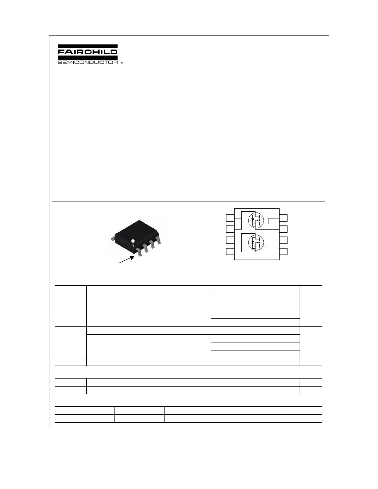
Dual 30V P-Channel PowerTrench MOSFET
May 2001
General Description
This P-Channel MOSFET is a rugged gate version of
Fairchild Semiconductor’s advanced PowerTrench
process. It has been optimized for power management
applications requiring a wide range of gave drive
voltage ratings (4.5V – 25V).
Applications
• Power management
• Load switch
• Battery protection
D1
D
D1
D
D2
D
D2
D
S2
S
G2
S
G1
G
S1
S
o
=25
C unless otherwise noted
A
SO-8
SO-8
Pin 1
Absolute Maximum Ratings T
Features
• –2.9 A, –30 V R
R
• Low gate charge (2.5nC typical)
• Fast switching speed
• High performance trench technology for extremely
low R
• High power and current handling capability
DS(ON)
5
6
7
8
= 130 mΩ @ VGS = –10 V
DS(ON)
= 200 mΩ @ VGS = –4.5 V
DS(ON)
4
Q1
Q2
3
2
1
Symbol Parameter Ratings Units
V
Drain-Source Voltage
DSS
V
Gate-Source Voltage
GSS
ID Drain Current – Continuous (Note 1a)
– Pulsed
PD
TJ, T
STG
Power Dissipation for Dual Operation 2
Power Dissipation for Single Operation (Note 1a) 1.6
(Note 1b)
(Note 1c)
Operating and Storage Junction Temperature Range –55 to +150 °C
–30
±25
±2.9
±10
1
0.9
V
V
A
W
Thermal Characteristics
R
Thermal Resistance, Junction-to-Ambient (Note 1a) 78 °C/W
θJA
R
Thermal Resistance, Junction-to-Case (Note 1) 40 °C/W
θJC
Package Marking and Ordering Information
Device Marking Device Reel Size Tape width Quantity
FDS9953A FDS9953A 13’’ 12mm 2500 units
2001 Fairchild Semiconductor Corporation FDS9953A Rev B(W)
FDS9953A
Electrical Characteristics T
= 25°C unless otherwise noted
A
Symbol Parameter Test Conditions Min Typ Max Units
Off Characteristics
BV
DSS
∆BVDSS
∆TJ
I
Zero Gate Voltage Drain Current
DSS
I
Gate–Body Leakage, Forward
GSSF
I
GSSR
Drain–Source Breakdown
Voltage
Breakdown Voltage Temperature
Coefficient
Gate–Body Leakage, Reverse
VGS = 0 V, ID = –250 µA
ID = –250 µA, Referenced to 25°C
VDS = –24 V, VGS = 0 V –2
VGS = –25 V, VDS = 0 V –100 nA
VGS = 25 V, VDS = 0 V 100 nA
–30 V
–23
mV/°C
µA
On Characteristics (Note 2)
V
Gate Threshold Voltage
GS(th)
∆VGS(th)
∆TJ
R
DS(on)
Gate Threshold Voltage
Temperature Coefficient
Static Drain–Source
On–Resistance
VDS = VGS, ID = –250 µA
ID = –250 µA, Referenced to 25°C
VGS = –10 V, ID = –1 A
VGS = –10 V, ID = –1 A, TJ=125°C
VGS = –4.5 V, ID = –0.5 A
VGS = –4.5 V, ID = –0.5 A, TJ=125°C
I
On–State Drain Current
D(on)
VGS = –10 V, VDS = –5 V –5
VGS = –4.5 V, VDS = –5 V –1.5
gFS Forward Transconductance VDS = –15 V, ID = –1 A 4 S
–1 –1.8 –3.0 V
4
95
137
142
202
130
200
200
310
mV/°C
m Ω
A
Dynamic Characteristics
C
Input Capacitance 185 pF
iss
C
Output Capacitance 56 pF
oss
C
Reverse Transfer Capacitance
rss
VDS = –15 V, V
f = 1.0 MHz
= 0 V,
GS
26 pF
Switching Characteristics (Note 2)
t
Turn–On Delay Time 4.5 9 ns
d(on)
tr Turn–On Rise Time 13 23 ns
t
Turn–Off Delay Time 11 20 ns
d(off)
tf Turn–Off Fall Time
Qg Total Gate Charge 2.5 3.5 nC
Qgs Gate–Source Charge 0.8 nC
Qgd Gate–Drain Charge
VDD = –15 V, ID = –1 A,
VGS = –10 V, R
GEN
= 6 Ω
VDS = –5 V, ID = –1 A,
VGS = –10 V
2 4 ns
0.9 nC
Drain–Source Diode Characteristics and Maximum Ratings
IS Maximum Continuous Drain–Source Diode Forward Current
VSD Drain–Source Diode Forward
VGS = 0 V, IS = –1.3 A (Note 2) –0.8 1.3 V
Voltage
trr Reverse Recovery Time VGS = 0 V, IF = –1.25A,
dIF/dt = 100A/µs
–1.2
A
17 100 nS
FDS9953A Rev B(W)
 Loading...