

Fairchild Semiconductor FDS9926A Datasheet
FDS9926A
Dual N-Channel 2.5V Specified PowerTrench MOSFET
FDS9926A
January 2000
PRELIMINARY
General Description
These N-Channel 2.5V specified MOSFETs use
Fairchild Semiconductor’s advanced PowerTrench
process. It has been optimized for power management
applications with a wide range of gate drive voltage
(2.5V – 10V).
Applications
Battery protection
•
Load switch
•
Power management
•
Features
6.5 A, 20 V. R
•
Optimized for use in battery protection circuits
•
allows for wide operating voltage range
10 V
• ±
GSS
Low gate charge
•
= 0.030 Ω @ VGS = 4.5 V
DS(ON)
= 0.043 Ω @ VGS = 2.5 V.
R
DS(ON)
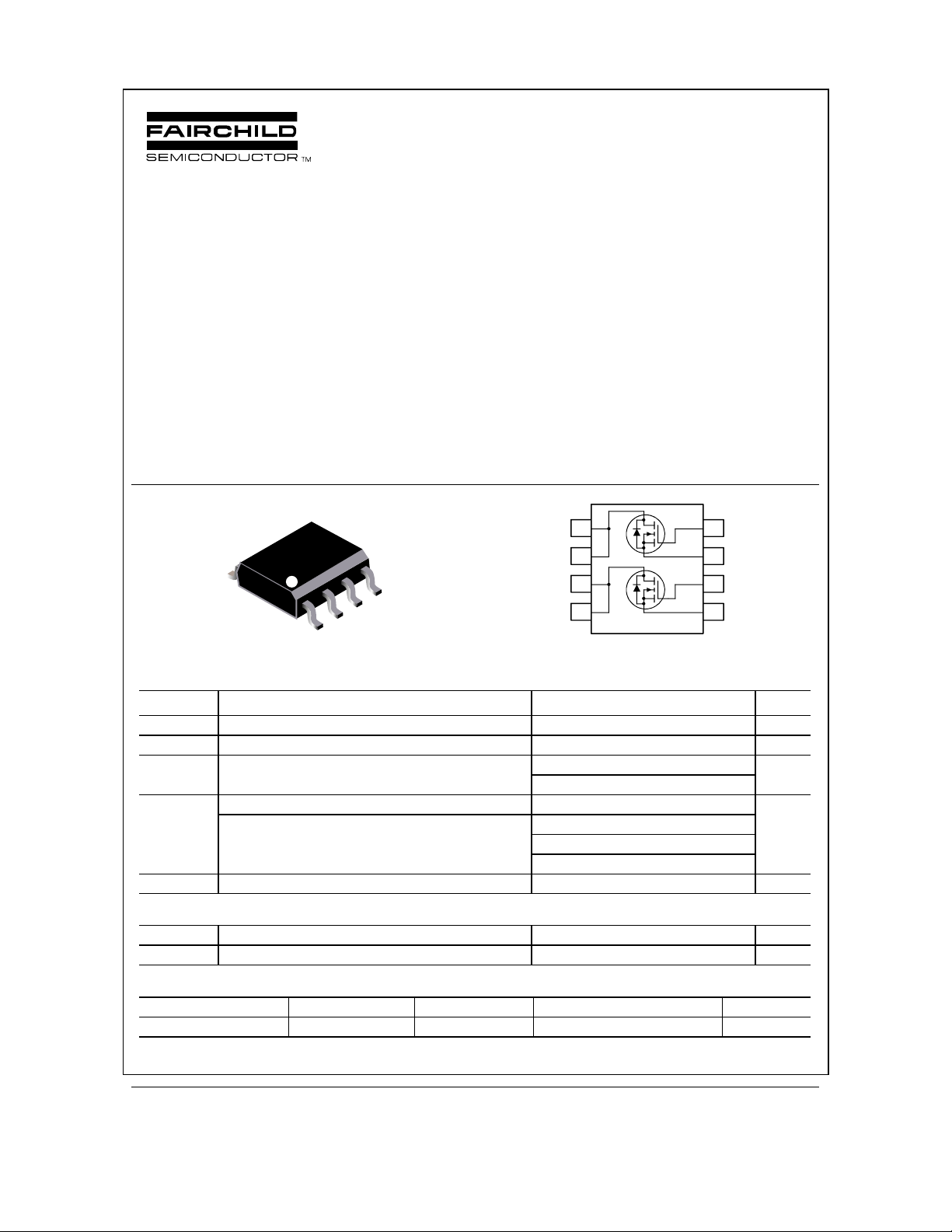
D1
D1
D2
D2
G1
S2
S1
G2
SO-8
Absolute Maximum Ratings
TA=25oC unless otherwise noted
5
Q1
6
7
Q2
8
4
3
2
1
Symbol Parameter Ratings Units
V
DSS
V
GSS
I
D
P
D
TJ, T
STG
Drain-Source Voltage 20 V
Gate-Source Voltage
Drain Current – Continuous
(Note 1a)
10
±
6.5 A
– Pulsed 20
Power Dissipation for Dual Operation 2
Power Dissipation for Single Operation
(Note 1a)
(Note 1b)
(Note 1c)
1.6
1
0.9
Operating and Storage Junction Temperature Range -55 to +150
V
W
C
°
Thermal Characteristics
R
JA
θ
R
JC
θ
Thermal Resistance, Junction-to-Ambient
Thermal Resistance, Junction-to-Case
(Note 1a)
(Note 1)
78
40
Package Marking and Ordering Information
Device Marking Device Reel Size Tape width Quantity
FDS9926A FDS9926A 13’’ 12mm 2500 units
1999 Fairchild Semiconductor Corpor ation
C/W
°
C/W
°
FDS9926A Rev C (W)
FDS9926A
Electrical Characteristics
TA = 25°C unless otherwise noted
Symbol Parameter Test Conditions Min Typ Max Units
Off Characteristics
BV
DSS
BV
∆
T
∆
I
DSS
I
GSSF
I
GSSR
On Characteristics
V
GS(th)
GS(th)
V
∆
T
∆
R
DS(on)
I
D(on)
g
FS
Drain–Source Breakdown Voltage
DSS
Breakdown Voltage Temperature
Coefficient
J
V
= 0 V, ID = 250 µA
GS
= 250 µA, Referenced to 25°C
I
D
20 V
14
Zero Gate Voltage Drain Current VDS = 16 V, VGS = 0 V 1
Gate–Body Leakage, Forward VGS = 8 V, VDS = 0 V 100 nA
Gate–Body Leakage, Reverse VGS = –8 V VDS = 0 V –100 nA
(Note 2)
Gate Threshold Voltage
Gate Threshold Voltage
Temperature Coefficient
J
Static Drain–Source
On–Resistance
V
= VGS, ID = 250 µA
DS
I
= 250 µA, Referenced to 25°C
D
VGS = 4.5 V, ID = 6.5 A
= 2.5 V, ID = 5.4 A
V
GS
= 4.5 V, ID =6.5A, TJ=125°C
V
GS
0.5 1 1.5 V
-3
0.025
0.036
0.035
On–State Drain Current VGS = 4.5 V, VDS = 5 V 15 A
Forward Transconductance VDS = 5 V, ID = 3 A 11 S
mV/°C
mV/°C
0.030
0.043
0.050
Dynamic Character istics
C
iss
C
oss
C
rss
Switching Characteristics
t
d(on)
t
r
t
d(off)
t
f
Q
g
Q
gs
Q
gd
Input Capacitance 700 pF
Output Capacitance 175 pF
Reverse Transfer Capacitance
(Note 2)
Turn–On Delay Time 8 16 ns
Turn–On Rise Time 10 18 ns
= 10 V, V
V
DS
f = 1.0 MHz
= 10 V, ID = 1 A,
V
DD
= 4.5 V, R
V
GS
GS
GEN
= 0 V,
= 6
85 pF
Ω
Turn–Off Delay Time 18 29 ns
Turn–Off Fall Time
Total Gate Charge 7 10 nC
Gate–Source Charge 1.2 nC
V
= 10 V, ID = 3A,
DS
V
= 4.5 V
GS
Gate–Drain Charge
510ns
1.9 nC
Drain–Source Diode Characteristics and Maximum Ratings
I
S
V
SD
Notes:
is the sum of the junction-to-case and case-to-ambient thermal resistance where the case thermal reference is defined as the solder mounting surface of
R
1.
JA
θ
the drain pins. R
Maximum Continuous Drain–Source Diode Forward Current 1.3 A
Drain–Source Diode Forward
VGS = 0 V, IS = 1.3 A
(Note 2)
0.65 1.2 V
Voltage
is guaranteed by design while R
JC
θ
is determined by the user's board design.
CA
θ
A
µ
Ω
a) 78°/W when
mounted on a 0.5in
pad of 2 oz copper
Scale 1 : 1 on letter size paper
Pulse Test: Pulse Width < 300µs, Duty Cycle < 2.0%
2.
2
b) 125°/W when
mounted on a 0.02
in2 pad of 2 oz
copper
c) 135°/W when mounted on a
minimum pad.
FDS9926A Rev C (W)
Typical Characteristics
FDS9926A
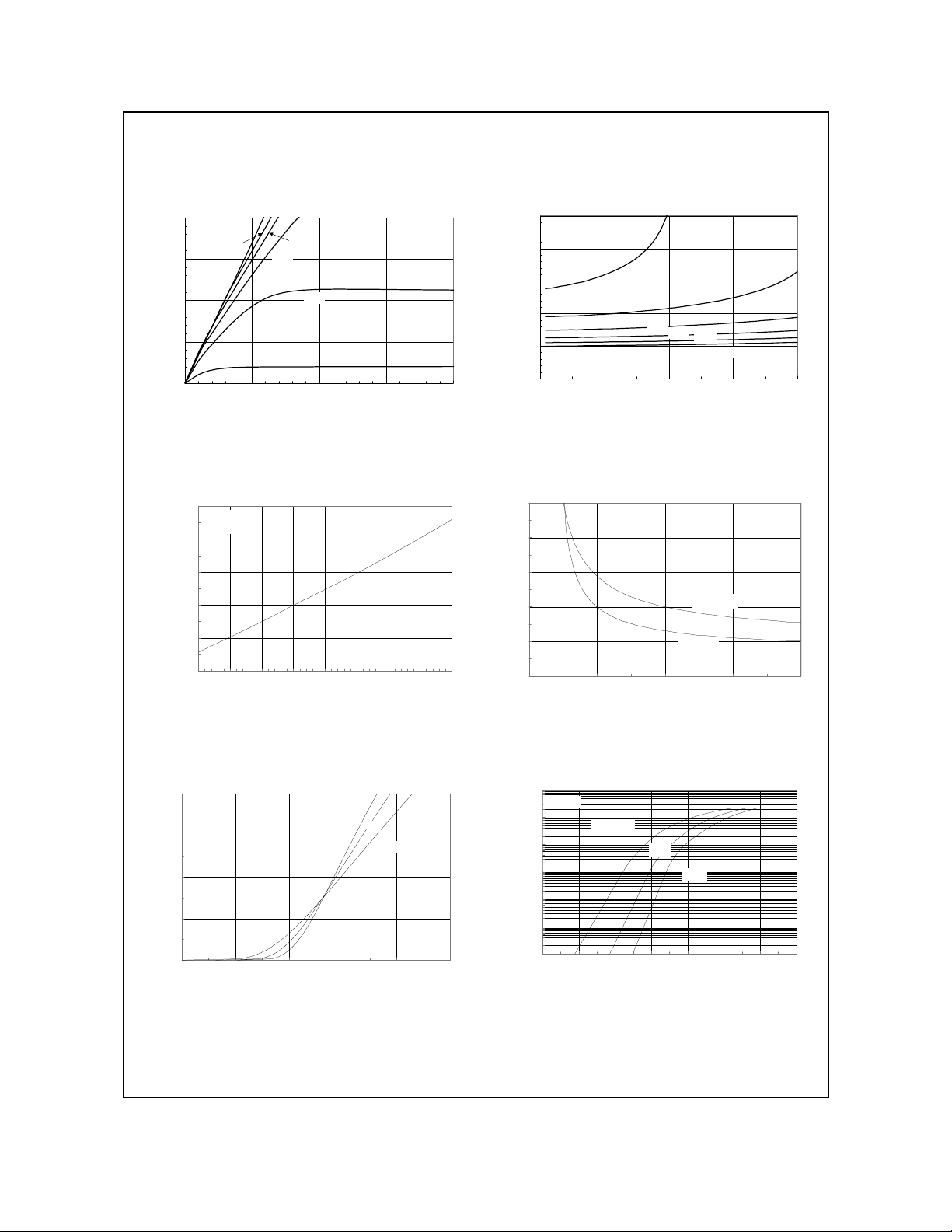
20
VGS = 4.5V
15
10
, DRAIN CURRENT (A)
5
D
I
0
3.5V
0 0.5 1 1.5 2
3.0V
2.5V
2.0V
1.5V
, DRAIN-SOURCE VOLTAGE (V )
V
DS
3
2.5
, NORMALIZED
1.5
DS(ON)
R
DRAIN-SOURCE ON-RESISTANCE
0.5
VGS = 2.0V
2
2.5V
3.0V
3.5V
1
0 5 10 15 20
I
, DRAIN CURRENT (A)
D
4.0V
Figure 1. On-Region Characteristics. Figure 2. On-Resistance Variation with
Drain Current and Gate Voltage.
1.6
ID = 3A
V
= 4.5V
GS
1.4
1.2
, NORMALIZED
1
DS(ON)
R
0.8
DRAIN-SOURCE ON-RESISTANCE
0.6
-50 -25 0 25 50 75 100 125 150
, JUNCTION TEMPERATURE (oC)
T
J
0.1
0.08
0.06
0.04
, ON-RESISTANCE (OHM)
0.02
DS(ON)
R
0
12345
, GATE TO SOURCE VOLTAGE (V)
V
GS
TA = 125oC
TA = 25oC
4.5V
ID = 1.5 A
Figure 3. On-Resistance Variation with
Temperature.
20
VDS = 5V
15
10
, DRAIN CURRENT (A)
5
D
I
0
0.511.522.53
V
, GATE TO SOURCE VOLTAGE (V)
GS
TA = -55oC
25
125oC
Figure 4. On-Resistance Variation with
Gate-to-Source Voltage.
100
VGS = 0V
10
1
0.1
0.01
0.001
, REVERSE DRAIN CURRENT (A)
S
I
0.0001
0 0.2 0.4 0.6 0.8 1 1.2 1.4
TA = 125oC
25oC
-55oC
, BODY DIODE FORWARD VOLTAGE (V)
V
SD
Figure 5. Transfer Characteristics. Figure 6. Body Diode Forward Voltage Variation
with Source Current and Temperature.
FDS9926A Rev C (W)
 Loading...