

Fairchild Semiconductor FDS4072N7 Datasheet
May 2003
FDS4072N7
40V N-Channel PowerTrench MOSFET
FDS4072N7
General Description
This N-Channel MOSFET has been designed
specifically to improve the overall efficiency of DC/DC
converters using either synchronous or conventional
switching PWM controllers. It has been optimized for
“low side” synchronous rectifier operation, providing an
extremely low R
in a small package.
DS(ON)
Applications
• Synchronous rectifier
Features
• 12.4 A, 40 V R
R
• High performance trench technology for extremely
DS(ON)
low R
• High power and current handling capability
• Fast switching
= 11 mΩ @ VGS = 4.5 V
DS(ON)
= 9 mΩ @ VGS = 10 V
DS(ON)
• DC/DC converter
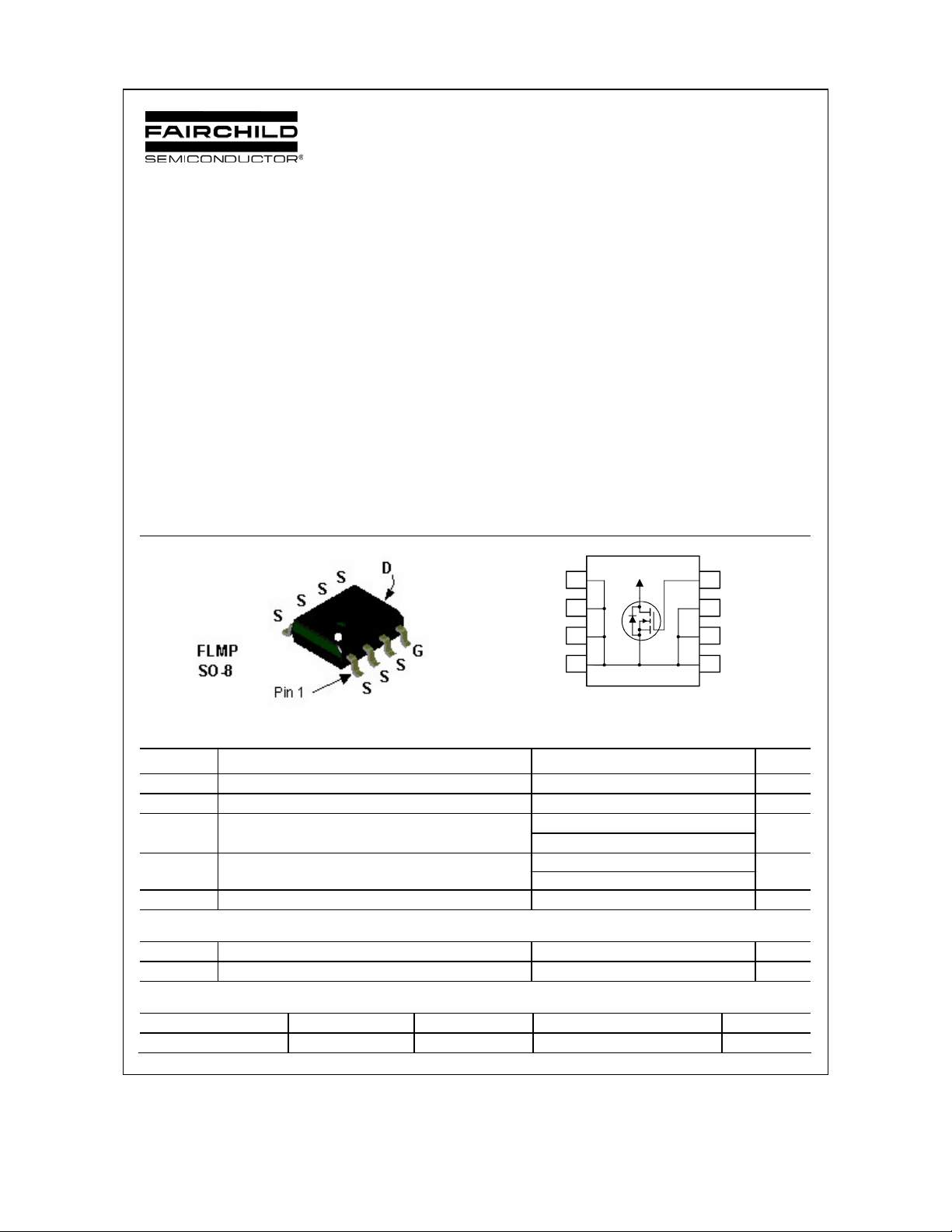
• FLMP SO-8 package: Enhanced thermal
performance in industry-standard package size
Bottom-side
Drain Contact
5
6
7
8
4
3
2
1
Absolute Maximum Ratings T
o
=25
C unless otherwise noted
A
Symbol Parameter Ratings Units
V
Drain-Source Voltage 40 V
DSS
V
Gate-Source Voltage
GSS
± 12
ID Drain Current – Continuous (Note 1a) 12.4 A
– Pulsed 60
PD
TJ, T
STG
Power Dissipation (Note 1a)
(Note 1b)
Operating and Storage Junction Temperature Range –55 to +150
3.0
1.5
V
W
°C
Thermal Characteristics
R
θJA
R
θJC
Thermal Resistance, Junction-to-Ambient
Thermal Resistance, Junction-to-Case
(Note 1a) 40
0.5
Package Marking and Ordering Information
Device Marking Device Reel Size Tape width Quantity
FDS4072N7 FDS4072N7 13’’ 12mm 2500 units
2002 Fairchild Semiconductor Corpora tion
FDS4072N7 Rev C1 (W)
°C/W
°C/W
FDS4072N7
Electrical Characteristics T
= 25°C unless otherwise noted
A
Symbol Parameter Test Conditions Min Typ Max Units
Drain-Source Avalanche Ratings (Note 2)
EAS Drain-Source Avalanche Energy Single Pulse, VDD = 20V, ID=12.4 A 200 mJ
IAS Drain-Source Avalanche Current 12.4 A
Off Characteristics
BV
Drain–Source Breakdown Voltage
DSS
∆BVDSS
∆T
I
Zero Gate Voltage Drain Current VDS = 32 V, VGS = 0 V 1
DSS
I
GSSF
I
GSSR
Breakdown Voltage Temperature
Coefficient
J
Gate–Body Leakage, Forward VGS = 12 V, VDS = 0 V 100 nA
Gate–Body Leakage, Reverse VGS = –12 V , VDS = 0 V –100 nA
= 0 V, ID = 250 µA
V
GS
= 250 µA, Referenced to 25°C
I
D
40 V
38
mV/°C
µA
On Characteristics (Note 2)
V
Gate Threshold Voltage
GS(th)
∆VGS(th)
∆TJ
R
DS(on)
Gate Threshold Voltage
Temperature Coefficient
Static Drain–Source
On–Resistance
I
On–State Drain Current VGS = 5 V, VDS = 5 V 30 A
D(on)
= VGS, ID = 250 µA
V
DS
= 250 µA, Referenced to 25°C
I
D
VGS = 4.5 V, ID = 12.4 A
= 10 V, ID = 13.7 A
V
GS
= 4.5 V, ID = 12.4 A,TJ = 125°C
V
GS
gFS Forward Transconductance VDS = 10 V, ID = 12.4 A 84 S
1 1.3 3 V
–4.5
9
8
14
11
9
18
mV/°C
mΩ
Dynamic Characteristics
C
Input Capacitance 4299 pF
iss
C
Output Capacitance 351 pF
oss
C
Reverse Transfer Capacitance
rss
V
= 20 V, V
DS
f = 1.0 MHz
= 0 V,
GS
149 pF
Switching Characteristics (Note 2)
= 20 V, ID = 1 A,
V
t
Turn–On Delay Time 20 36 ns
d(on)
tr Turn–On Rise Time 12 22 ns
t
Turn–Off Delay Time 52 83 ns
d(off)
tf Turn–Off Fall Time
Qg Total Gate Charge 33 46 nC
Qgs Gate–Source Charge 7.8 nC
Qgd Gate–Drain Charge
DD
= 4.5 V, R
V
GS
= 20 V, ID = 12.4 A,
V
DS
= 4.5 V
V
GS
GEN
= 6 Ω
18 32 ns
8.1 nC
Drain–Source Diode Characteristics and Maximum Ratings
IS Maximum Continuous Drain–Source Diode Forward Current 2.5 A
VSD
trr Diode Reverse Recovery Time 30 nS
Qrr Diode Reverse Recovery Charge
Drain–Source Diode Forward
Voltage
= 0 V, IS = 2.5 A (Note 2) 0.7 1.2 V
V
GS
= 12.4 A,
I
F
= 100 A/µs
d
iF/dt
90 nC
FDS4072N7 Rev C1 (W)
FDS4072N7
Electrical Characteristics T
Notes:
1. R
is the sum of the junction-to-case and case-to-ambient thermal resistance where the case thermal reference is defined as the solder mounting surface of
θJA
the drain pins. R
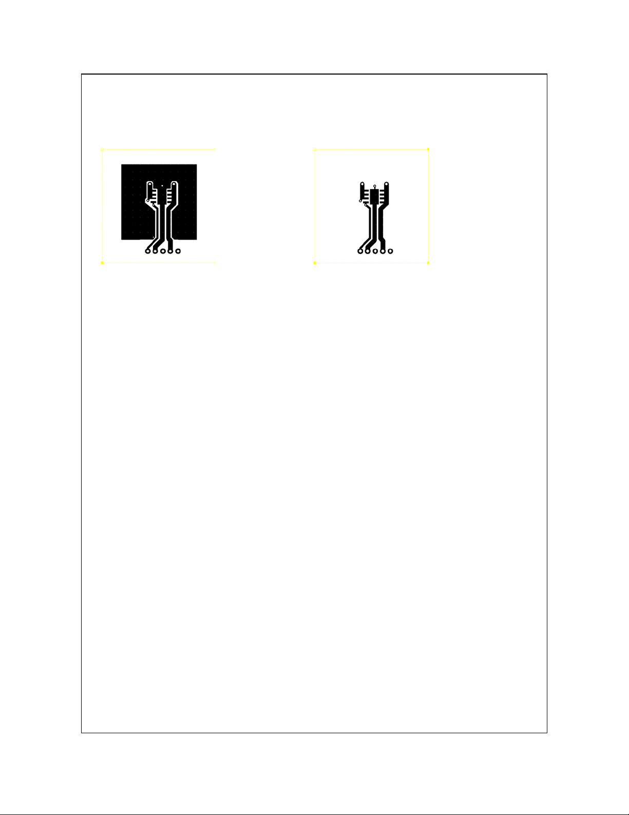
Scale 1 : 1 on letter size paper
2. Pulse Test: Pulse Width < 300µs, Duty Cycle < 2.0%
is guaranteed by design while R
θJC
is determined by the user's board design.
θCA
a) 40°C/W when mounted
on a 1in2 pad of 2 oz
copper
= 25°C unless otherwise noted
A
b) 85°C/W when mounted on
a minimum pad of 2 oz
copper
FDS4072N7 Rev C1 (W)
 Loading...