

Fairchild Semiconductor FDS3912 Datasheet
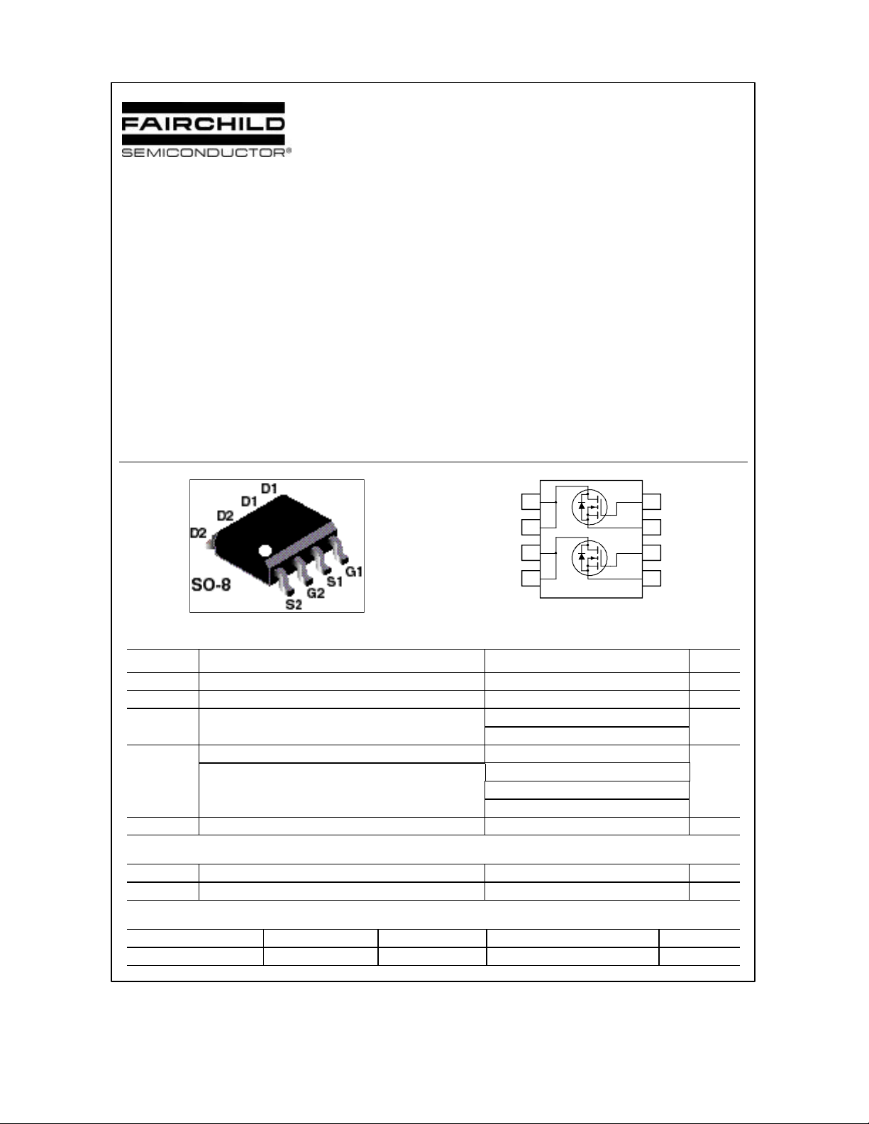
FDS3912
FDS3912
100V Dual N-Channel PowerTrench MOSFET
October 2001
General Description
These N-Channel MOSFETs have been designed
specifically to improve the overall efficiency of DC/DC
converters using either synchronous or conventional
switching PWM controllers.
These MOSFETs feature faster switching and lower
gate charge than other MOSFETs with comparable
R
specifications. The result is a MOSFET that is
DS(ON)
easy and safer to drive (even at very high frequencies),
and DC/DC power supply designs with higher overall
efficiency.
Features
• 3 A, 100 V. R
R
• Fast switching speed
• Low gate charge (14 nC typ)
• High performance trench technology for extremely
low R
DS(ON)
= 125 mΩ @ VGS = 10 V
DS(ON)
= 135 mΩ @ VGS = 6 V
DS(ON)
• High power and current handling capability
4
3
2
1
Absolute Maximum Ratings T
=25oC unless otherwise noted
A
5
Q1
6
7
Q2
8
Symbol Parameter Ratings Units
V
DSS
V
GSS
I
D
P
D
TJ, T
STG
Drain-Source Voltage 100 V
Gate-Source Voltage ±20 V
Drain Current – Continuous (Note 1a) 3 A
– Pulsed 20
Power Dissipation for Dual Operation 2
Power Dissipation for Single Operation (Note 1a) 1.6
(Note 1b)
(Note 1c)
1.0
0.9
Operating and Storage Junction Temperature Range –55 to +175
W
°C
Thermal Characteristics
R
θJA
R
θJC
Thermal Resistance, Junction-to-Ambient (Note 1a) 78
Thermal Resistance, Junction-to-Case (Note 1) 40
Package Marking and Ordering Information
Device Marking Device Reel Size Tape width Quantity
FDS3912 FDS3912 13’’ 12mm 2500 units
2001 Fairchild Semiconductor Corporation
°C/W
°C/W
FDS3912 Rev C2(W)
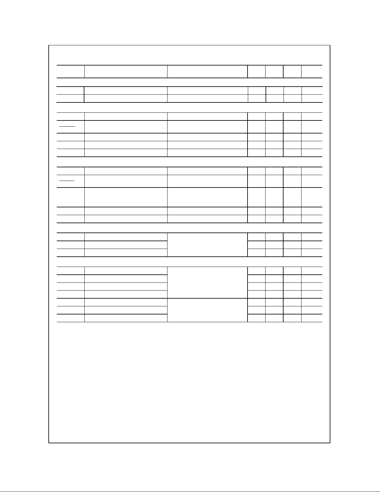
Electrical Characteristics T
FDS3912
= 25°C unless otherwise noted
A
Symbol Parameter Test Conditions Min Typ Max Units
Drain-Source Avalanche Ratings (Note 2)
W
DSS
I
AR
Drain-Source Avalanche Energy Single Pulse, VDD = 50 V, ID= 3 A 90 mJ
Drain-Source Avalanche Current 3.0 A
Off Characteristics
BV
DSS
∆BVDSS
∆T
I
DSS
I
GSSF
I
GSSR
Drain–Source Breakdown Voltage
Breakdown Voltage Temperature
Coefficient
J
VGS = 0 V, ID = 250 µA
ID = 250 µA,Referenced to 25°C
100 V
108
Zero Gate Voltage Drain Current VDS = 80 V, VGS = 0 V 10
Gate–Body Leakage, Forward VGS = 20 V, VDS = 0 V 100 nA
Gate–Body Leakage, Reverse VGS = –20 V, VDS = 0 V –100 nA
mV/°C
µA
On Characteristics (Note 2)
V
GS(th)
∆VGS(th)
∆T
R
DS(on)
I
D(on)
g
FS
Gate Threshold Voltage
Gate Threshold Voltage
Temperature Coefficient
J
Static Drain–Source
On–Resistance
VDS = VGS, ID = 250 µA
ID = 250 µA,Referenced to 25°C
VGS = 10 V, ID = 3 A
VGS = 6 V, ID = 2.8 A
V
= 10 V, ID = 3 A, TJ = 125°C
GS
2 2.5 4 V
–6
92
98
175
On–State Drain Current VGS = 10 V, VDS = 10 V 10 A
Forward Transconductance VDS = 10V, ID = 3 A 11 S
125
135
250
mV/°C
mΩ
Dynamic Characteristics
C
iss
C
oss
C
rss
Input Capacitance 632 pF
Output Capacitance 40 pF
Reverse Transfer Capacitance
VDS = 50 V, V
f = 1.0 MHz
GS
= 0 V,
20 pF
Switching Characteristics (Note 2)
t
t
t
t
Q
Q
Q
d(on)
r
d(off)
f
g
gs
gd
Turn–On Delay Time 8.5 17 ns
Turn–On Rise Time 2 4 ns
VDD = 50 V, ID = 1 A,
VGS = 10 V, R
GEN
= 6 Ω
Turn–Off Delay Time 23 37 ns
Turn–Off Fall Time
Total Gate Charge 14 20 nC
Gate–Source Charge 2.4 nC
VDS = 50 V, ID = 3 A,
VGS = 10 V
Gate–Drain Charge
4.5 9 ns
3.8 nC
FDS3912 Rev C2(W)
 Loading...