

Fairchild Semiconductor FDH600 Datasheet
FDH / FDLL 600
Discrete POWER & Signal
Technologies
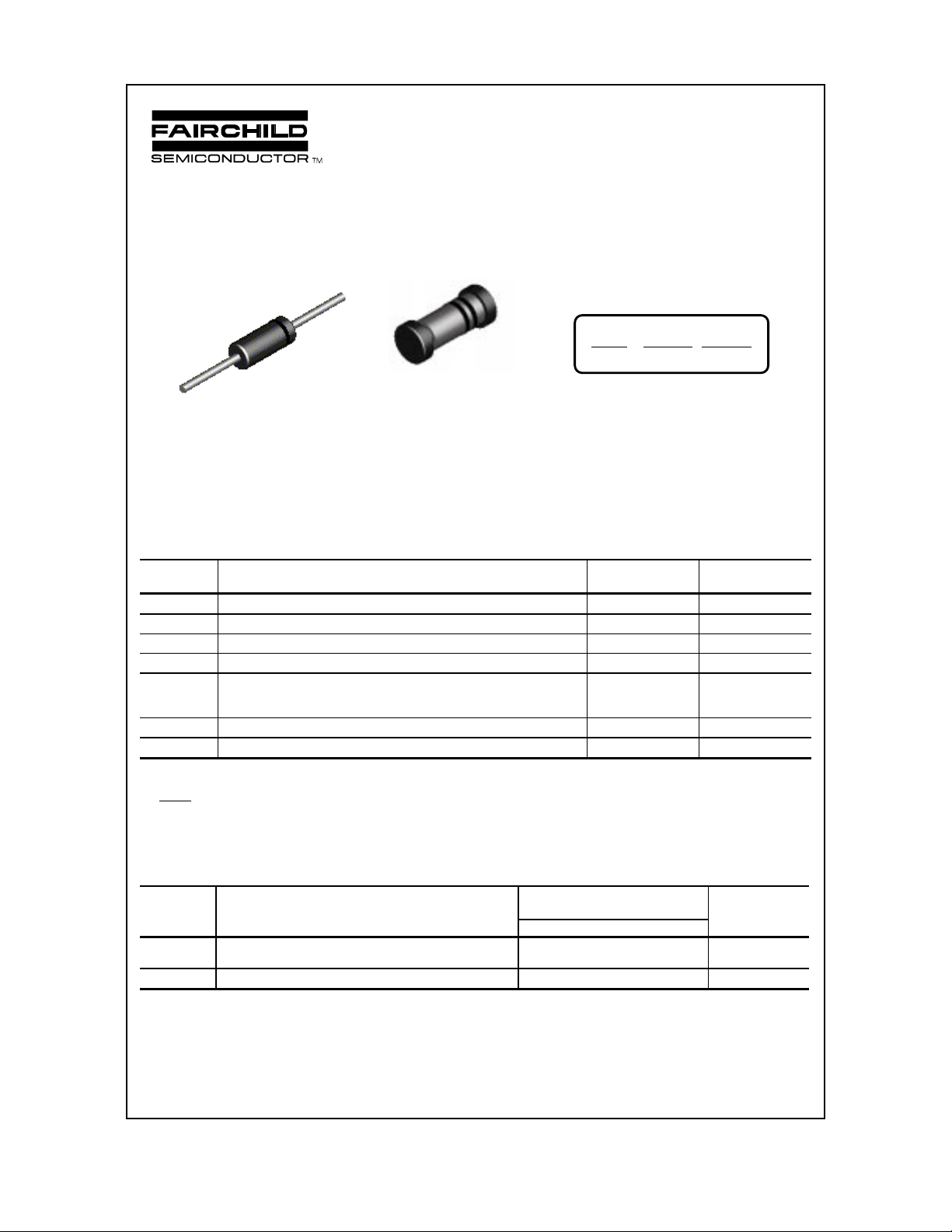
COLOR BAND MARKING
DEVICE
FDLL600 RED WHITE
1ST BAND 2ND BAND
FDH600 / FDLL600
LL-34
DO-35
THE PLACEMENT OF THE EXPANSION GAP
HAS NO RELATIONSHIP TO THE LOCATION
OF THE CATHODE TERMINAL
High Conductance Ultra Fast Diode
Sourced from Process 1R. See MMBD1201-1205 for characteristics.
Absolute Maximum Ratings* TA = 25°C unless otherwise noted
Symbol Parameter Value Units
W
IV
I
O
I
F
i
f
i
f(surge)
T
stg
T
J
*These ratings are limiting values above which the serviceability of any semiconductor device may be impaired.
NOTES:
1) These ratings are based on a maximum junction temperature of 200 degrees C.
2) These are steady state limits. The factory should be consulted on applications involving pulsed or low duty cycle operations.
Working Inverse Voltage 50 V
Average Rectified Current 200 mA
DC Forward Current 400 mA
Recurren t Peak Forward Current 600 mA
Peak Forward Surge Current
Pulse width = 1.0 second
Pulse width = 1.0 microsecond
Storage Temperature Range -65 to +200
Operating Junction Temperature 175
1.0
4.0
A
A
°
°
C
C
Thermal Characteristics TA = 25°C unless otherwise noted
Symbol Characteristic Max Units
FDH/FDLL 600
P
D
R
θ
JA
ã 1997 Fairchild Semiconductor Corporation
Total Dev ice Dissipation
Derate above 25°C
500
3.33
Thermal Resistan ce, Junction to Ambient 300
mW
mW/°C
C/W
°
µ
High Conductance Ultra Fast Diode
(continued)
Electrical Characteristics TA = 25°C unless otherwise noted
Symbol Parameter Test Conditions Min Max Units
B
V
I
R
V
F
C
O
T
RR
Breakdown Voltage
I
= 5.0 µA
R
Reverse Current VR = 50 V
= 50 V, TA = 150°C
V
R
Forward Voltage IF = 1.0 mA
I
= 10 mA
F
I
= 50 mA
F
I
= 100 mA
F
I
= 200 mA
F
75 V
100
100
650
790
860
920
mV
mV
mV
mV
1.0
nA
Diode Capacitance VR = 0, f = 1.0 MHz 2.5 pF
Reverse Recovery Time
I
= IR = 10 mA, I
F
R
= 100
Ω
L
= IR = 200 mA, I
I
F
R
= 100
Ω
L
= 1.0 mA,
rr
= 20 mA,
rr
4.0
6.0
nS
nS
A
V
FDH600 / FDLL600
 Loading...