

Fairchild Semiconductor FAN5066 Datasheet

www.fairchildsemi.com
FAN5066
Ultra Low Voltage Synchronous DC-DC Controller
Features
• Output adjustable from 400mV to 3.5V
• Synchronous Rectification
• Adjustable operation from 80KHz to 1MHz
• Integrated Power Good and Enable functions
• Overvoltage protection
• Overcurrent protection
• Drives N-channel MOSFETs
• 20 pin SOIC or TSSOP package
Applications
• Power supply DDR SDRAM VTT
• Power Supply HSTL
• Power Supply for ASICs
• Adjustable ultra-low voltage step-down power supply
Block Diagram
Description
The FAN5066 is a synchronous mode DC-DC controller IC
which provides an adjustable output voltage for ultra-low
voltage applications, down to 400mV. The FAN5066 uses a
high level of integration to deliver load currents in excess of
19A from a 5V source with minimal external circuitry.
Synchronous-mode operation offers optimum efficiency over
the entire output voltage range, and the internal oscillator
can be programmed from 80KHz to 1MHz for additional
flexibility in choosing external components. The FAN5066
also offers integrated functions including a four-bit
DAC-controlled reference, Power Good, Output Enable,
over-voltage protection and current limiting.
+12V
FAN5066
1
OSC
–
+
–
–
+
16
CNTRL
20
VREF
PRELIMINARY INFORMATION describes products that are not in full production at the time of printing. Specifications are based on design goals
and limited characterization. They may change without notice. Contact Fairchild Semiconductor for current information.
4-BIT
DAC
19 18 17 8 2
VID2 VID4
VID1
VID3
REFERENCE
+
1.24V
DIGITAL
CONTROL
ENABLE
–
+
POWER
GOOD
5
4
13
12
7
9
3
+5V
+5V
VO
PWRGD
REV. 2.1.4 11/13/01

FAN5066 PRODUCT SPECIFICATION
Pin Assignments
CEXT
ENABLE
PWRGD
IFB
VFB
VCCA
VCCP
VID4
LODRV
GNDP
1
2
3
4
5
FAN5066
6
7
8
912
10 11
VREF
20
VID1
19
VID2
18
VID3
17
CNTRL
16
15
GNDA
GNDD
14
VCCQP
13
HIDRV
GNDP
Pin Definitions
Pin Number Pin Name Pin Function Description
1 CEXT Oscillator Capacitor Connection . Connecting an external capacitor to this pin sets
the internal oscillator frequency. Layout of this pin is critical to system performance.
See Application Information for details.
2 ENABLE Output Enable . A logic LOW on this pin will disable the output. An internal pull-up
resistor allows for either open collector or TTL compatibility.
3 PWRGD Power Good Flag . An open collector output that will be at logic LOW if the output
voltage is not within ± 12% of the nominal output voltage setpoint.
4 IFB
5 VFB
6 VCCA Analog VCC . Connect to system 5V supply and decouple with a 0.1 µ F ceramic
7 VCCP Power VCC for low side FET driver . Connect to system 5V supply and place a 1 µ F
8 VID4
9 LODRV Low Side FET Driver . Connect this pin to the gate of an N-channel MOSFET for
10, 11 GNDP Power Ground . Return pin for high currents flowing in pins 7 and 13 (VCCP and
12 HIDRV High Side FET Driver . Connect this pin to the gate of an N-channel MOSFET. The
13 VCCQP Power VCC . For high side FET driver. VCCQP must be connected to a voltage of at
14 GNDD Digital Ground . Return path for digital logic. Connect to a low impedance system
15 GNDA Analog Ground . Return path for low power analog circuitry. This pin should be
16 CNTRL Voltage Control . The voltage forced on this pin determines the output voltage of the
17-19 VID1-VID3 Voltage Identification Code Inputs . These open collector/TTL compatible inputs will
20 VREF Reference Voltage Test Point . This pin provides access to the DAC output and should
High Side Current Feedback . Pins 4 and 5 are used as the inputs for the current
feedback control loop. Layout of these traces is critical to system performance. See
Application Information for details.
Voltage Feedback . Pin 5 is used as the input for the voltage feedback control loop and
as the low side current feedback input. See Application Information for details regarding
correct layout.
capacitor.
ceramic capacitor for decoupling and local charge storage.
VID4 Input . A logic 1 on this open collector/TTL input will enable the VID3–VID0 inputs
to set the output from 2.1V to 3.5V, and a logic 0 will set the output from 1.3V to 2.05V,
as shown in Table 1. Pullup resistors are internal to the controller.
synchronous operation. The trace from this pin to the MOSFET gate should be < 0.5".
VCCQP). Connect to a low impedance ground.
trace from this pin to the MOSFET gate should be < 0.5".
least VCCA + V
(MOSFET), and place a 1 µ F ceramic capacitor for decoupling
GS,ON
and local charge storage. See Application Information for details
ground plane to minimize ground loops.
connected to a low impedance system ground plane to minimize ground loops.
converter.
program the output voltage of the reference over the ranges specified in Table 1.
Pull-up resistors are internal to the controller.
be decoupled to ground using 0.1µF capacitor.
2
REV. 2.1.4 11/13/01

°
•
±
•
•
PRODUCT SPECIFICATION FAN5066
Absolute Maximum Ratings
Supply Voltages, VCCA, VCCP, VCCQP to GND 13V
Supply Voltage VCCQP, Charge Pump (V
+VCCA) 18V
IN
Voltage Identification Code Inputs, VID3-VID0 13V
VREF Output Current 3mA
Junction Temperature, T
J
150 ° C
Storage Temperature -65 to 150 ° C
Lead Soldering Temperature, 10 seconds 300 ° C
Operating Conditions
Parameter Conditions Min. Typ. Max. Units
Supply Voltage, VCCA, VCCP 4.75 5 5.25 V
Input Logic HIGH 2.0 V
Input Logic LOW 0.8 V
Ambient Operating Temp 0 70
Output Driver Supply, VCCQP 8.5 12 V
C
Electrical Specifications
(V
= 5V, V
CCA
The • denotes specifications which apply over the full operating temperature range.
Parameter Conditions Min. Typ. Max. Units
Initial Voltage Setpoint I
Output Temperature Drift T
Load Regulation I
Line Regulation V
Output Ripple 20MHz BW, I
DAC Output Voltage See Table 1 1.3 3.4 V
DAC Accuracy -3 +3 %
Short Circuit Detect Threshold
Output Driver Rise and Fall Time See Figure 3 80 nsec
Output Driver Deadtime 1 See Figure 3 5 %/f
Output Driver Deadtime 2 See Figure 3 80 nsec
Turn-on Response Time I
Oscillator Range 80 1000 KHz
Oscillator Frequency C
PWRGD threshold Logic High
PWRGD Minimum Operating
Voltage
Max Duty Cycle 90 95 %
Control Pin Input Current V
CNTRL
= 900mV, f
= 300 KHz, and T
osc
= 0.8A, V
LOAD
= 0 to 70 ° CV
A
= 0.8A to 3A
LOAD
= 4.75V to 5.25V
IN
= 0A to 3A 10 msec
LOAD
= 100 pF 270 300 330 KHz
EXT
Logic Low
= 400mV to 3.5V
CTRL
= +25 ° C using circuit in Figure 1, unless otherwise noted)
A
CTRL
V
CTRL
V
OUT
OUT
= 1.25V
= 900mV
= 1.25V
= 900mV
1.237
891
•
•
1.250
900
+6
+4
1.263
909
-20 mV
LOAD
•±
= 3A
2mV
13 mVpk
90 120 150 mV
93
88
107
112
1.0 V
235 µA
%V
%V
V
mV
mV
mV
OSC
OUT
OUT
REV. 2.1.4 11/13/01
3
FAN5066 PRODUCT SPECIFICATION
Table 1. DAC Output Voltage Programming Codes
VID4 VID3 VID2 VID1 V
0111 1.30V
0110 1.40V
0101 1.50V
0100 1.60V
0011 1.70V
0010 1.80V
0001 1.90V
0000 2.00V
1111 No Output
1110 2.2V
1101 2.4V
1100 2.6V
1011 2.8V
1010 3.0V
1001 3.2V
1000 3.4V
REF
Note:
1. 0 = processor pin is tied to GND.
1 = processor pin is open.
4
REV. 2.1.4 11/13/01

PRODUCT SPECIFICATION FAN5066
Typical Operating Characteristics
(VCCA, VCCD = 5V, f
= 280 KHz, and T
OSC
= +25 ° C using circuit in Figure 1, unless otherwise noted)
A
80
70
60
50
40
Efficiency (%)
30
20
0.1 0.3 0.6 0.9 1.2 1.5 1.8 2.1 2.4 2.7 3
Output Current (A)
Output Voltage vs. Output Current,
Efficiency vs. Output Current
R
= 6mΩ
SENSE
1.4
1.2
1.0
0.8
(V)
0.6
OUT
V
0.4
0.2
0
0 1 2 3 4 5
Output Current (A)
(V)
OUT
V
Load Regulation V
0.895
0.890
0.885
0.880
0.875
0.870
OUT
0 0.5 1 1.5 2 2.5 3
Output Current (A)
Oscillator Frequency vs. C
1250
1050
850
650
450
Frequency (KHz)
250
50
18 39 75 150 300 560
C
(pf)
EXT
= 0.9V
EXT
REV. 2.1.4 11/13/01
5
FAN5066 PRODUCT SPECIFICATION
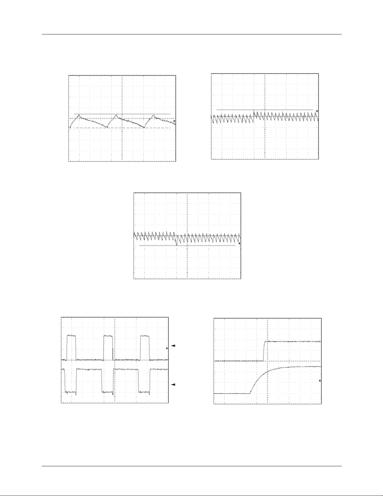
Typical Operating Characteristics
Output Ripple, 900m @ 3A
(20mV/div)
OUT
V
Time (1µs/division)
Transient Response, 0.1A to 3A
(continued)
(20mV/div)
OUT
V
Transient Response, 3A to 0.1A
Time (10µs/division)
Switching Waveforms, 3A Load Output Startup, System Power-up
2V/div 5V/div
(20mV/div)
OUT
V
Time (1µs/division)
Time (1µs/division)
HIDRV
pin
LODRV
pin
(500mV/div)
OUT
(2V/div ) V
IN
V
Time (5ms/division)
65-5051-12
6
REV. 2.1.4 11/13/01
 Loading...