Fairchild Semiconductor FAN4822 Datasheet

www.fairchildsemi.com
FAN4822
ZVS Average Current PFC Controller
Features
• Average current sensing, continuous boost, leading edge
PFC for low total harmonic distortion and near unity
power factor
• Built-in ZVS switch control with fast response for high
efficiency at high power levels
• A verage line v oltage compensation with bro wnout control
• Current fed gain modulator improves noise immunity and
provides universal input operation
• Overvoltage comparator eliminates output “runaway” due
to load removal
• UVLO, current limit, and soft-start
• Precision 1.3% reference
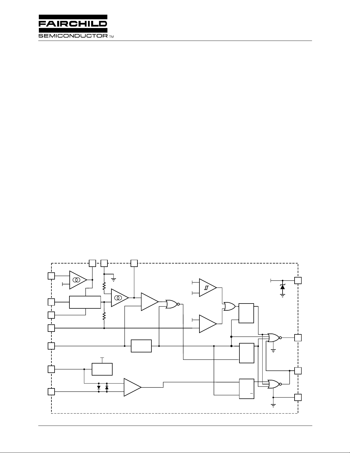
Block Diagram
1
14
13
4
5
3
6
FB
2.5V
I
AC
V
RMS
I
SENSE
R
TCT
REF
VEAO
VEA
–
+
GAIN
MODULATOR
R+
R–
V
REF
CCZ
8
GND
+
–
IEA
2
IEAO
+
–
OSC
General Description
The FAN4822 is a PFC controller designed specifically for
high power applications. The controller contains all of the
functions necessary to implement an average current boost
PFC converter, along with a Zero Voltage Switch (ZVS) controller to reduce diode recovery and MOSFET turn-on
losses.
The average current boost PFC circuit provides high power
factor (>98%) and low Total Harmonic Distortion (THD).
Built-in safety features include undervoltage lockout, overvoltage protection, peak current limiting, and input voltage
brownout protection.
The ZVS control section drives an external ZVS MOSFET
which, combined with a diode and inductor, soft switches the
boost regulator. This technique reduces diode reverse recovery and MOSFET switching losses to reduce EMI and maximize efficiency.
V
CC
12
PFC OUT
11
ZVS OUT
10
FB
2.7V
–1V
+
–
I LIMIT
+
–
OVP
SRQ
SRQ
V
CCZ
13.5V
Q
ZV SENSE
7
+
––
QS
R
Q
PWR GND
9
REV. 1.0.1 8/10/01

FAN4822 PRODUCT SPECIFICATION
Pin Configuration
FAN4822
16-Pin SOIC (S16W)
1
2
3
4
5
6
7
8
TOP VIEW
14-Pin DIP (P14)
VEAO
IEAO
I
SENSE
I
AC
V
RMS
RTC
ZV SENSE
T
Pin Description
FAN4822
1
2
3
4
5
6
7
TOP VIEW
14
13
12
11
10
9
8
FB
REF
V
CC
PFC OUT
ZVS OUT
PWR GND
GND
VEAO
IEAO
I
SENSE
I
V
RMS
RTC
ZV SENSE
N/C
AC
T
(Pin numbers is parentheses are for 16-pin package)
Pin Name Function
1 (1) VEAO Transconductance voltage error amplifier output.
2 (2) IEAO Transconductance current error amplifier output.
3 (3) I
SENSE
4 (4) I
5 (5) V
6 (6) R
AC
RMS
C
T
T
Current sense input to the PFC current limit comparator.
PFC gain modulator reference input.
Input for RMS line voltage compensation.
Connection for oscillator frequency setting components.
7 (7) ZV SENSE Input to the high speed zero voltage crossing comparator.
8 (10) GND Analog signal ground.
9 (11) PWR GND Return for the PFC and ZVS driver outputs.
10 (12) ZVS OUT ZVS MOSFET driver output.
11 (13) PFC OUT PFC MOSFET driver output.
12 (14) V
CC
Shunt-regulated supply voltage.
13 (15) REF Buffered output for the internal 7.5V reference.
14 (16) FB Transconductance voltage error amplifier input.
16
15
14
13
12
11
10
9
FB
REF
V
CC
PFC OUT
ZVS OUT
PWR GND
GND
N/C
Absolute Maximum Ratings
Absolute maximum ratings are those values beyond which the device could be permanently damaged. Absolute maximum ratings are stress ratings only and functional device operation is not implied.
Parameter Min Max Unit
Shunt Regulator Current (I
Peak Driver Output Current ±500 mA
Analog Inputs –0.3 7 V
Junction Temperature 150 °C
Storage Temperature Range –65 150 °C
Lead Temperature (Soldering, 10 sec) 150 °C
Thermal Resistance ( θ
Plastic DIP
Plastic SOIC
2
)55mA
CC
)
JA
80
110
°C/W
°C/W
REV. 1.0.1 8/10/01

∆
∆
∆
∆
Ω
PRODUCT SPECIFICATION FAN4822
Operating Conditions
Temperature Range Min. Max. Units
FAN4822IX –40 85 °C
Electrical Characteristics
Unless otherwise specified, R
Parameter Conditions Min. Typ. Max. Units
Voltage Error Amplifier
Input Voltage Range 0 7 V
Transconductance V
Feedback Reference Voltage V
Open Loop Gain 60 75 dB
PSRR V
Output Low 0.65 1 V
Output High 6.0 6.7 V
Source Current
Sink Current
Current Error Amplifier
Input Voltage Range –1.5 2 V
Transconductance V
Input Offset Voltage ±3 ±15 mV
Open Loop Gain 60 75 dB
PSRR V
Output Low 0.65 1 V
Output High 6.0 6.7 V
Source Current
Sink Current
OVP Comparator
Threshold Voltage 2.6 2.7 2.8 V
Hysteresis 80 120 150 mV
I
SENSE
Comparator
Threshold Voltage –0.8 –1.0 –1.15 V
Delay to Output 150 300 ns
ZV Sense Comparator
Propagation Delay 100mV Overdrive 50 ns
Threshold Voltage 7.35 7.5 7.65 V
Input Capacitance 6 pF
= 52.3k Ω , C
T
NON-INV
EAO
CCZ
V
IN
V
IN
NON-INV
CCZ
V
IN
V
IN
= 470pF, T
T
= V
INV
= V
FB
– 3V < V
= ±0.5V, V
= ±0.5V, V
= V
INV
– 3V < V
= ±0.5V, V
= ±0.5V, V
= Operating Temperature Range (Note 1)
A
, VEAO = 3.75V 50 70 120
2.4 2.5 2.6 V
CC
OUT
OUT
< V
– 0.5V 60 75 dB
CCZ
= 6V –40 –80 µA
= 1.5V 40 80 mA
, IEAO = 3.75V 130 195 310
CC
OUT
OUT
< V
– 0.5V 60 75 dB
CCZ
= 6V –30 –80 µ A
= 1.5V 40 80 µ A
µ
µ
Ω
REV. 1.0.1 8/10/01
3
 Loading...